1. The Usual High Speed PCB Layout Rules
You still need to follow all the rules that would apply to digital logic speeds reaching over 100 MHz. Remember, 100+ MHz digital logic carries 1GHz components too, because square waves contain higher order harmonics.
Therefore, the following rules will always apply:
- Do not run MIPI DSI traces across gaps in ground plane.
- No split ground plane anywhere that interrupts the return current path under MIPI DSI traces.
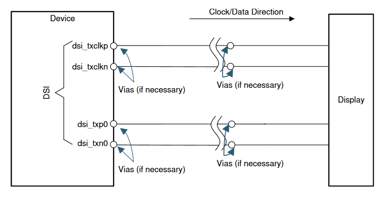
- Avoid having vias between a differential pair if you can.
- Avoid using vias to carry MIPI DSI signals to other layers if possible. Using vias should be a last choice.
- The maximum clock that you will see on a MIPI DSI interface is 500 MHz, therefore it is important to shield these lines from other pairs and other electronics nearby that can be affected, such as WiFi or BT chipsets or antennas.
2. Controlled Impedance Traces
Single ended impedance: 50 ohms (tolerance: +/- 15%)
Differential impedance: 90 ohms (tolerance: +/- 15%)
On a typical 1.6mm FR4 PCB with 7628 type stackup (4 layers), the above specifications usually result in 4.5 mil wide traces with about 6 mils of gap between the traces. This can vary, make sure you calculate it using an online impedance calculator or similar tool.
3. Reference Plane
MIPI DSI bus reference plane can be GROUND or POWER.
This means that you can use vias to route DSI lines on the bottom side of a 4-layer board without worrying about signal integrity problems.
NOTE that you need to add 10nF capacitors on both sides of the lines between POWER and GROUND for handling return currents on change of reference plane.
4. Length Matching and Constraints
0.15 mm or 5 mils
1.5 mm or 50 mils
200 mm or 7800 mils
None allowed
Please fill in the Subscription Form in the sidebar so we can keep you updated with our latest articles.
We only mail you less than 2 times a month.
Change Log
- Initial Release: 23 May 2021
References
- Reference 1: Toradex Design Guide
- Reference 2: Texas Instruments SPRACP4