RP2040 PCB design procedure and difficulty level should be approximately similar to designing a custom PCB for STM32 series of MCUs. The RP2040 from Raspberry Pi does not differ a whole lot from most ARM Cortex-M0+ MCUs available in the market. There are a few basic differences though that need consideration when designing a custom board for the RP2040.
Here are some things worth keeping in mind, based on my experience of designing RP2040 boards.
What is Different with RP2040 PCB Design?
Cortex-M0+ MCUs offered by ST Micro (STM32G0 series) are quite similar to the RP2040, but there are key differences and these will come into consideration when designing a PCB with RP2040. The most important things that make RP2040 different are:
- Dual Core
This makes the RP2040 consume slightly more power than an STM32 single core Cortex M0+ would. However, the additional power consumption is not something you need to worry about. We have noticed the worst case current consumption to be ~40 mA. - SPI Flash for Code and Data Storage
The mandatory SPI flash adds a step to the PCB design process. You need to make sure that the SPI flash is connected properly with the RP2040. The traces must be routed properly to ensure low radiated noise from the high speed SPI lines. - Tiny QFN package only
QFN packages can be hard to solder for someone who is a hobbyist and does not have access to good quality soldering tools. QFN MCU package forces you to use tiny SMD parts to go with it.
Power Supply for RP2040
The power supply requirements for RP2040 are minimal, thanks to the low power consumption of the chip. However, an important thing to note is that the RP2040 requires 2 voltage supplies to operate: 3.3V for peripherals and ~1V for the core.
The 1V core supply or DVDD can be derived by the RP2040 itself using the 3.3V VREG_VIN. However, this is not too efficient beacuse the internal LDO operates at a very low efficiency. You might want to consider powering the DVDD lines from a switching converter if the RP2040 is usually active but runs off a battery pack.
If you are not too concerned about battery life or the RP2040 only runs for brief periods, the internal LDO for producing DVDD is good enough.
Finally, do not forget the decoupling capacitors! The RP2040 is dual core with an external code memory (flash) – which means tons of noise if you do not do the decoupling right.
Place decoupling caps as close as possible to all power pins that need decoupling (consult hardware design guide listed in references below).
RP2040 SPI Flash PCB Layout
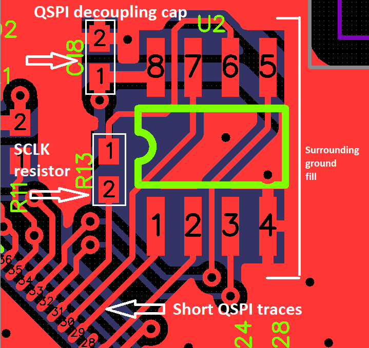
The quad SPI or QSPI flash is a high speed chip. Care needs to be taken to ensure that the PCB design takes that into account. Bad trace layout can cause corrupt read/write cycles and interference with other active components of the RP2040 PCB layout.
A few things to watch out for when drawing the schematics:
- RP2040 only supports a maximum of 16 MByte or 128 MBit SPI flash.
- If possible, you need to stick to using a flash chip that is compatible with W25Q128JVS. Chips from different manufacturers may have different commands sets – which adds to the risk of your design not working if you use another SPI flash memory.
When laying out the PCB:
- Try to keep the QSPI flash close to the RP2040. The maximum trace length being shorter than 1 inch is ideal. 8 mil trace width is good.
- Clock trace should be the longest trace among all the RP2040 to QSPI signals.
- It is always a good idea to add a series termination resistor on the SPI clock line. The value can be 0 ohms, or between 10 ohms to 100 ohms if required.
- Try to have a solid ground plane connecting the ground of the flash chip to the exposed pad of the RP2040.
External Crystal for RP2040
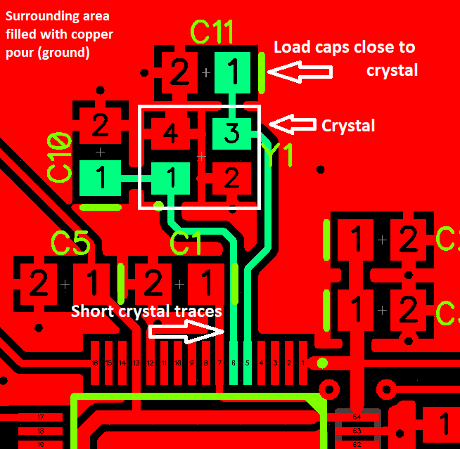
Crystal oscillator signals are quite weak and need to be protected from interference. When laying out clock/oscillator signals:
- Make sure the crystal load capacitors are according to the crystal datasheet.
- Load capacitors for the crystal must be located close to the crystal itself.
- Traces connecting RP2040 and the crystal should be short and away from other high speed traces nearby (like the QSPI traces).
- You can skip the crystal altogether if you can rely on the rather unstable internal oscillator. However, it is always best to leave an empty footprint in case you change your mind later!
USB Traces for RP2040
USB traces on the RP2040 are not really “high speed” provided that the RP2040 integrates a USB 1.1 phy that can do 1.5 Mbps in Low Speed Mode and 12 Mbps in Full Speed Mode.
The USB lines are sampled at 48 MHz.
Given that this USB interface is nowhere close to the 480 Mbps USB 2.0 interface that STM32 and many other Cortex-M series MCUs offer, you can relax on the USB routing restrictions here.
If the USB traces are shorter than 1 inch, you can use 6 to 8 mil wide traces, with D+ and D- routed close together.
If you are running longer traces, you can use an online microstrip impedance calculator [ref. 2] and make sure that D+ and D- lines have
- Single ended impedance: 50 ohms, +/- 15%
- Differential impedance: 90 ohms, +/- 15%
- Length mismatch between D+ and D- traces should be less than 100 mils.
Audio ADC, DAC, or Codec with RP2040
Audio circuits can be a pain to lay out and end up with the clean audio you want to achieve.
In general, audio output does not get noisy easily. For example, if you are driving headphones or speakers via an audio DAC or codec with the RP2040, your PCB design will need to be absolutely terrible to cause noise. Minor mistakes will not cause audible noise in playback.
However, audio recording is prone to noise because the microphone and any other audio capture device will always generate weak signals. This means that the signal is easily contaminated by noise sources on the RP2040 PCB.
Some tips for avoiding noise when designing audio applications with RP2040:
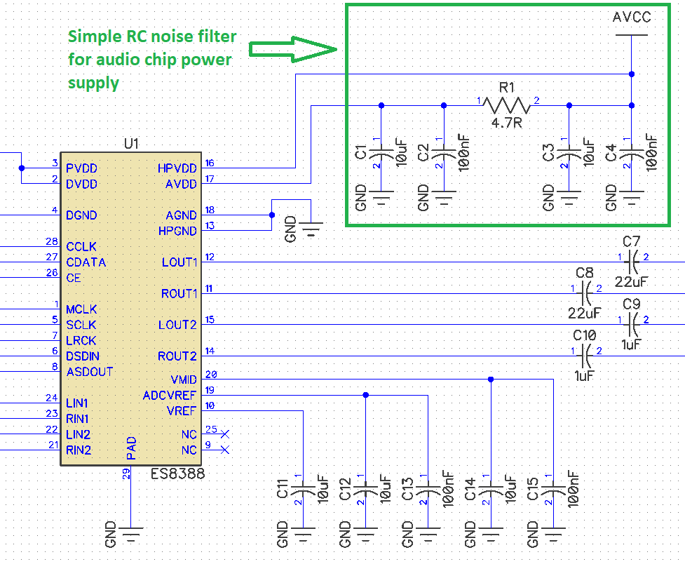
- Use a separate LDO for audio ADC, DAC or codec.
- Use sufficient decoupling and if needed, use filters on low power analog power pins of the audio chip.
- Use series resistors on the codec I2S lines and MCLK audio clock line to control digital noise.
- ALWAYS read the audio chip’s datasheet to ensure you have everything done right.
- Try and maintain a reasonably solid ground plane under the whole RP2040 PCB design. Use star routing for power lines if it is a 2 layer board.
SD Card PCB Layout
This part of the design is covered by the same guidelines that apply to the QSPI flash chip.
Camera Sensor with RP2040
Make sure to reasonably match the camera interface traces in length and they should be around 6 to 8 mils wide.
Trace length should be approximately equal for all of the following lines, with a length mismatch of less than 200 mils for:
- D[0] to D[n] for n data lines of the camera parallel port.
- VSYNC and HSYNC
- PCLK and any other clock lines
Other lines like camera sensor reset or enable, etc can be of any length.
Fill in the Quick Contact Form in the sidebar and we will get back to you ASAP!
Change Log
- Initial Release: 14 June 2021
References
- Reference 1: Hardware Design with RP2040
- Reference 2: PCBWay Trace Impedance Calculator
- Reference 3: RP2040 Datasheet