Chip antenna PCB layout can be tricky business, especially if you are new to RF PCB design. RF signals behave very differently when compared to digital or analog signals that you usually encounter in common embedded systems. These days with IoT applications gaining massive popularity and market share, RF layout becomes important.
This article covers some basics of using chip antenna for 2.4 GHz applications. Anything you read in this article will apply to single ended Wi-Fi and Bluetooth chip antennas.
Chip Antenna PCB Layout - What Really Matters
With a chip antenna, it is best to think of what matters as listed here, in the order of decreasing priority:
- What is under the antenna (ground plane and fill)
- Size of the ground plane
- The feed line and its characteristics
- What is near the antenna on the PCB (within 1 cm)
- Parts over or under the antenna (enclosure, battery, etc)
Now that you know that these play an important role when designing a PCB using a chip antenna, let me walk you through a more detailed description of each of these points.
1. Ground Plane and Fill under Chip Antenna
There will always be exceptions, but chip antennas do not like ground plane directly underneath them. Most chip antennas will require you to have a ground plane clearance under them on all layers. Manufacturers specify how much clearance is required and you should take the values exactly from the chip antenna datasheet.
Here is an example of a resonance cavity chip antenna PCB design that requires a specific ground clearance shape on all copper layers to work.
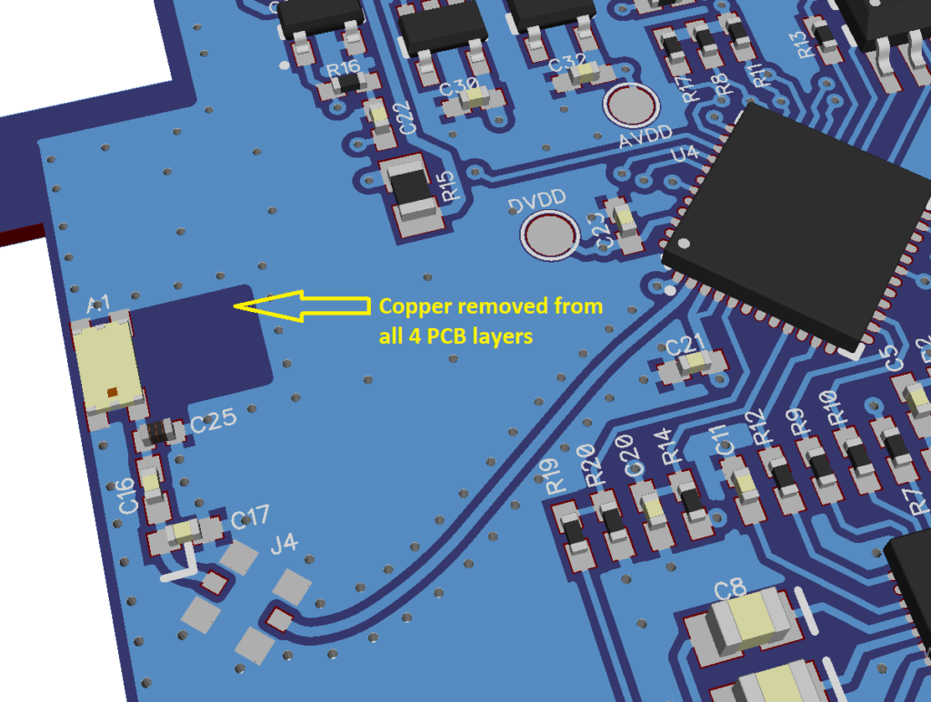
The ground fill around the chip antenna is extremely important for the antenna to function properly. You must stitch vias on the chip antenna ground plane fill edge. The vias should be stitched at 50 mil or smaller gap between vias, with a drill size of 14 mils or larger in case of 2.4 GHz signals. If a different stitch type is specified in the chip antenna datasheet, you should stick to it.
The point of stitching vias along the gound plane edge is to provide a solid, low impedance ground return path back to the RF MCU or SoC. This low impedance return path also makes sure that no RF energy interferes with other components on board.
2. Size of the PCB Ground Plane
Size of the ground plane matters when a PCB uses a chip antenna, especially for relatively high power communication like Wi-Fi. Antenova [Ref.1] has compiled a great article on why the size of ground plane matters in IoT applications.
A simple explanation towards why ground plane size matters is that dipole antennas have two radiators. However, a chip antenna is just one radiatior – which leaves the PCB ground plane to act as the second radiator – thus making the system act as a dipole antenna.
If you consider the wavelength of the band you are operating on, you need the PCB ground plane size to be at least a quarter of the wavelength of the baseband. That is how the ceramic chip antenna and PCB ground plane together make a half-wave dipole antenna.
If your system PCB does not meet that minimum length requirement, the chip antenna performance might suffer severely compared to the datasheet specifications (that are derived using an ideal PCB size).
3. Antenna Feed Line and Characteristics
The antenna feed line is extremely important. How would it not be? The trace is responsible for carrying transmitted and received signals. A bad feed line design not only affects transmission efficiency – it affects the receiver range too. If your feed trace is not 50 ohms and contains obstructions, it can detune the antenna, cause massive loss of RF signal strength both ways and ultmately reduce the range of the device drastically.
If the transmitter is a high power device radiating more than 500mW, poor feed line design or 90 degree bends can cause permanent damage to the RF SoC.
The feed line must be designed with these common guidelines in mind:
- Stick to a 50 ohm feed line.
If the SoC or RF PA output is not 50 ohms, you must use an RLC network as necessary to convert it to 50 ohms before using a long feed line. - The feed line should not have sharp bends or stubs on it.
Use a curved trace to bend the trace is needed. Avoiding bends is always preferable where possible. - Solid ground plane underneath feed line.
You need a solid ground plane underneath the feed line extending all the way to the RF chip’s ground pad. This ensures that the RF signals will return back to the chip via a low impedance ground path. - Never cut the ground plane under a feed line.
The feed line should NEVER jump over a gap in the reference ground plane below it. This can cause major problems. - Use small matching components that have pads as wide as the RF trace.
If the matching network component pads are larger in width than the RF feed line itself, the pads acts as stubs or capacitors and can affect the feed line characteristics. If you are forced to use large components, you might need to clear the ground plane from under the excess pad area to reduce prasitic capacitance (at least for inductors). - Avoid accidental stubs
This can be hard to spot, but if you have to branch your RF trace, always do it in a way that does not add stubs to the active branch of the feed line microstrip.
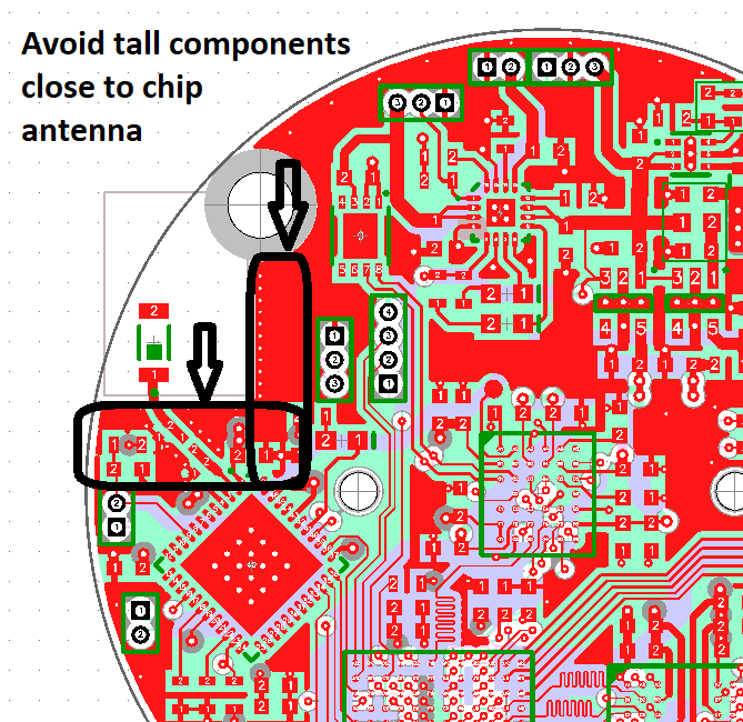
4. Components Near the Chip Antenna
Proximity of other electronics components to the chip antenna can cause problems in two ways:
- Radiated RF may cause glitches in other sensitive digial logic (MCU reset lines, high impedance digital inputs, floating op-amp inputs, etc).
- Metal components near the antenna can deform the antenna radiation pattern. This can result in omni-directional antennas not acting as expected.
Here is an illustration of what you should ideally do if there is a chip antenna involved.
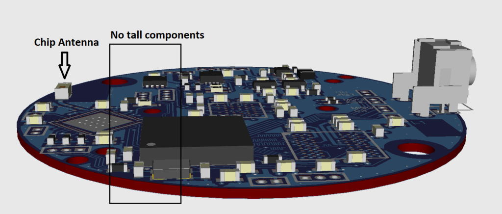
5. Parts Over and Under the Chip Antenna Zone
In case you need assistance with the implementation or tuning of chip antenna on a custom PCB, feel free to contact us.
Please fill in the Subscription Form in the sidebar so we can keep you updated with our latest articles.
We only mail you less than 2 times a month.
Change Log
- Initial Release: 04 June 2021
References
- Reference 1: Chip antenna performance on tiny PCBs
- Reference 2: Antenna implementation whitepaper