SDRAM pin swapping is a term used to refer to a variety of techniques used to simplify PCB design where an MCU and SDRAM are involved. SDRAM swapping rules can be used in a number of ways to avoid using several vias on a signal that is a part of the high speed memory bus. The primary types of pin swapping that you will find to be in use with SDR and DDR SDRAM chips are
- Data lane swapping or byte swapping
- Data line swapping or bit swapping
- Address line swapping
Swapping in SDR SDRAM vs DDR SDRAM
It is important to distinguish between regular SDR SDRAM and DDR memories.
Types of Swapping Usable with SDRAM
I listed the types of swapping options that are commonly used with PCB design involving SDRAM chips. Here is a closer look at why you can or cannot use a certain swap option.
Lane or Byte Swapping
Yes, you can do this with an SDR SDRAM chip. However, make sure that you have other related control pins swapped as well, for example the data lane mask pins for the two lanes must be swapped too.
For example, if you have a memory chip with 16-bit data bus, the data bus can be divided into bytes:
Byte 0: DQ[0] to DQ[7]
Byte 1: DQ[8] to DQ[15]
The byte 0 is sometimes called the lower data byte and marked as LD, while the upper byte is called the UD.
You can connect DQ[8] to DQ[15] of the MCU to the SDRAM memory chip’s DQ[0] to DQ[7] too without issues. Howevery, make sure you have the LDQM, UDQM and other such byte-specific signals swapped too.
Data Line or Bit Swapping
Yes, you can do this with an SDR SDRAM chip.
There are no restrictions on swapping of data lines inside a certain data byte. This swapping rule can be used in addition to the rule above.
Note that you cannot swap data lines between bytes, i.e. you can swap DQ[3] and DQ[6]. But you cannot swap DQ[2] with DQ[13].
The reason for this restriction should be obvious to you. The mask signals, LDQM and UDQM control a certain byte and therefore you cannot swap out lines outside a certain byte because the mask logic will fail.
NOTE: You should still double-check with your SDRAM datasheet to make sure that it has no special functions associated with a certain data bit. For example, DDR memories do not allow DQ[0] and DQ[8] to be swapped with any other bits because they are used for read/write leveling function.
Address Line Swapping
No, cannot do this with an SDR SDRAM chip.
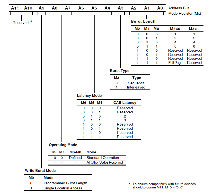
Now, you can compensate for this swap in firmware when you set the SDRAM memory up, but that still does not solve the problem.
Now you know the basics of what works and what to look for when it comes to interfacing between an MCU or FPGA and SDRAM memory chips.
It is ALWAYS recommended to consult the MCU or FPGA memory controller datasheet and the SDRAM chip datasheet before you finalize any hardware design!
Please fill in the Subscription Form in the sidebar so we can keep you updated with our latest articles.
We only mail you less than 2 times a month.
Change Log
- Initial Release: 23 May 2021
References
- Reference 1: ISSI IS42S16400J Datasheet
- Reference 2: Freescale AN2582
- Reference 3: Related Xilinx forum post
- Reference 4: Microchip AN3310, connecting SDR and DDR memories