i.MX6 DDR3 PCB layout can be a daunting task for someone who does not often design high speed PCBs. Also, because i.MX6 chips are quite similar across variants in many ways, these notes can apply to any chip of the series. I have put these notes down while designing an i.MX6 Solo X based custom PCB.
In short, this article is the set of notes that I use when routing i.MX6 boards. All the resources that are suggested reading material are linked in the references section below.
Optimal Placement for i.MX6 DDR3 PCB Layout
i.MX6 SoCs have all the DDR DRAM related balls on one side of the chip. The data lanes and data lane strobes are all along the outer edge of the chip and therefore it is possible to connect all the data lanes to the DDR chips using 2 layers of the PCB.
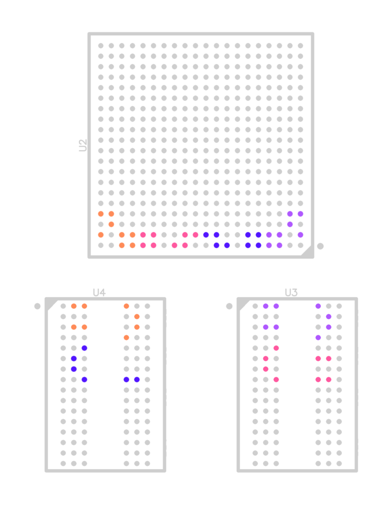
To figure out which data bus pin will connect to what DDR3 chip data lane, you can start with a simple data bus pin map. Here is a map for the i.MX6 Solo X chip and a couple of 2Gb DDR3L DRAM chips.
- Lay out differential data lane strobes on layer L1 and L3 for DDR3 on the left
- Lay out length matched data lane bits and DQM for DDR3 on the left
- Length match everything based on matching guidelines below
- Mirror this routing pattern over to the DDR3 on the right side
DDR3 Trace Length Matching Strategy
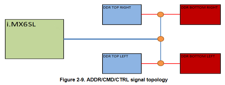
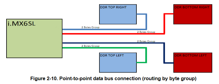
A T-topology is possible in a symmetric arrangement like this [ref.1]. We do not have a lot of DDR chips and capacitive loading should not really be a concern here with short signal trace lengths. In a case like this, the best way to route traces is as follows [ref.2].
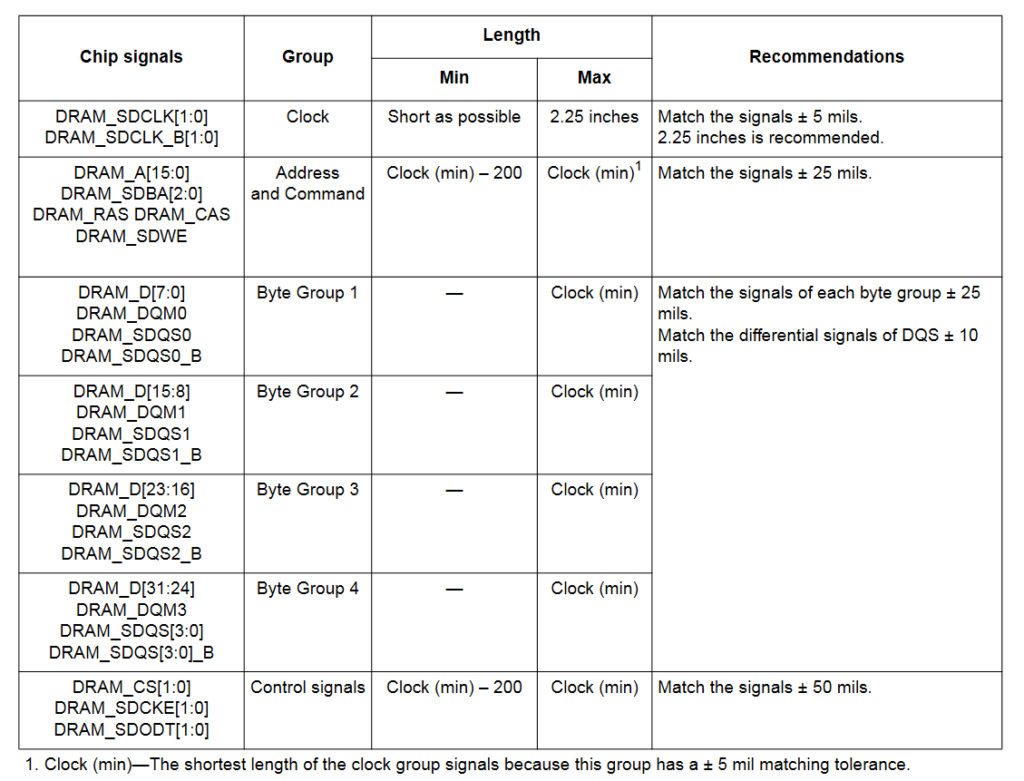
For the data lanes, length should be matched within a data lane. For i.MX6 Solo X, only two 2-byte groups are used for a 32-bit wide data bus.
DDR3 PCB Layout Length Matching Rules and Constraints
Please fill in the Subscription Form in the sidebar so we can keep you updated with our latest articles.
We only mail you less than 2 times a month.
Change Log
- Initial Release: 30 April 2021
References
- Reference 1: Whitepaper on DDR3 Routing Topologies
- Reference 2: i.MX6 Series Layout Recommendations
- Reference 3: i.MX6 Sabre OrCAD PCB Design Files