Common VGH, VGL, VCOM and AVDD voltage levels
TFT LCD panels always have a controller in there which is a CoG (chip on glass) type IC planted on to the panel to drive the rows and columns. The chip has referenace values and tables to drive the display to get the desired contrast and bias voltage needed to control the LCD pixels properly. Incorrect values can cause the panel to look low contrast and weak, or in the other extreme case cause permanent damage to the panel.
The CoG controller IC datasheet usually specifies a range of VGH, VGL, VCOM and AVDD values as absolute maximum rating. As a designer you must ensure that those values are not exceeded. Because the current draw is very little on VGH, VGL and VCOM, overshoots can be a problem in poorly designed circuits.
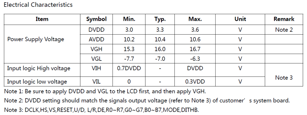
In addition to this, the LCD manufacturer configures the CoG LCD controller to use certain bias voltages that match the LCD panel characteristics (all LCD panels are not exactly the same). Here is an example from a 7″ display datasheet (ER-TFT07-2) with RGB interface.
In most cases, the VGH level is going to be less than twice the AVDD level. VGL magnitude will usually be less than AVDD as well, but it will be negative.
To generate all these power rails, one can simply use a single boost converter to generate AVDD and use the switching function to operate charge pumps that generate the other voltage rails. VGH and VGL rails do not draw a lot of current and are easy to regulate using “discrete” linear regulator circuits as we will describe in the next section.
Generating VGH, VGL, VCOM and AVDD
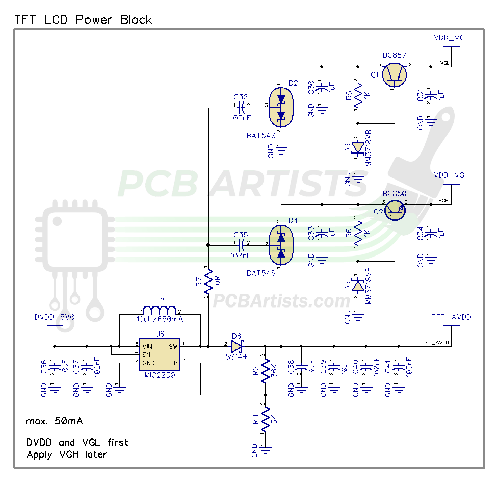
Zener diodes D3 and D5 help form basic linear regulators that regulate VGH and VGL. Using just zener diodes will also work. Many cheap designs use just zener diodes but it does increase power dissipation in the zener. Using a transistor and zener for linear regulation is a better option.
The value of the VGH and VGL decoupling capacitors can be modified to slightly trim power rail sequencing. We have not noticed any issues with using the same values for both VGH and VGL with most panels. However, if your panel requires strict power-on sequencing, you must take that into account by using a pass-transistor with delayed turn-on (or similar solution).
VCOM is not shown in thie schematic but it can be obtained by using a simple voltage divider on the AVDD rail. If you need a high current capacity on the VCOM rail, you can use an opamp in voltage follower configuration. In our case, we simply use the input 5V as the VCOM voltage often if VCOM = AVDD/2 and AVDD is about 10V.
How the circuit works
- The boost converter IC is responsible for generating AVDD and delivering a good load handling capacity on the AVDD rail. Nothing special here and a regular boost converter is used.
- Q2 forms the LDO that regulates the output of the charge pump formed by C35 and D4. The zener diode sets the output voltage and must be set correctly.
Output and input decoupling capacitors for this stage are important and you must pick a value that can keep the voltage output stable through the charge pump cycles. - Q1 and D3 form the negative voltage regulator. The negative voltage is generated by charge pump arrangement of C32 and D2. Again, the zener sets the voltage and decoupling capacitors are important.
- VCOM can either be supplied by the input 5V or extracted by dividing AVDD if the current requirement for VCOM is low (as is usually the case). If VCOM must handle heavy loads, an opamp voltage buffer works well.
- Digital supply rails for the display are not shown, but are derived from the LCD controller or application MCU (3.3V, usually).
Please fill in the Subscription Form in the sidebar so we can keep you updated with our latest articles.
We only mail you less than 2 times a month.
If you need assistance with hardware design involving TFT LCD displays, feel free to get in touch!
Change Log
- Initial Release: 07 March 2021
References
- Reference 1: ER-TFT070-2 documentation
- Reference 2: Waveshare LCD panel schematics
4 comments
Useful information.
Thanks for this article. Managed to fix a broken digital photo frame. Your example circuit almost matched directly to the power circuit on that board. With a few measurements I was able to deduce what the likely cause was. Removed the bad capacitor and got a working screen again!
Glad it helped! This is a very common arrangement for 10″ and smaller panels. The boost converter chips vary.
Just cleared many voltage type confusions.
Helpful!