STM32 series of microcontrollers suffer a major limitation – they lack on-chip SRAM, just like any other typical MCU. There is plenty of SRAM for your typical needs, but not enough to act as a frame buffer for camera or display.
Some STM32 MCUs do have external memory controllers, called FSMC or Flexible Static Memory Controller in SMT32 literature. They allow addition of external flash and SDRAM memory chips to extend the type of storage that you might need for your application.
Get the schematic right
Adding external SDRAM takes up a bunch of physical I/O pins on the microcontroller. This often ends up conflicting with other peripherals on the STM32, which prevents you from using certain other hardware features if you use the external memory controller. The TFT driver shares the memory controller pins on some STM32 MCUs. Make sure you rule out conflicting I/Os that might mess with SDRAM operation.
Most PCB layout tools will allow you to declare net class rules and restrictions in the schematic itself. It is a good idea to make use of that with the SDRAM lines so that you don’t have to look at them later in layout. I prefer to highlight them with a different color and declare length matching rules in schematic itself if the design has many different parallel data buses.
Layer stackup
Layer stackup is extremely important when laying out boards with external memory. A 2-layer board is a non-starter if you care at all about performance or EMI.
You can use a 4-layer board if you are experienced with PCB layout and both the STM32 and the SDRAM are provided in a non-BGA package.
If STM32 and SDRAM are BGA packages, 6 layers is the bare minimum that you need to route out the PCB properly without compromising on power or signal integrity.
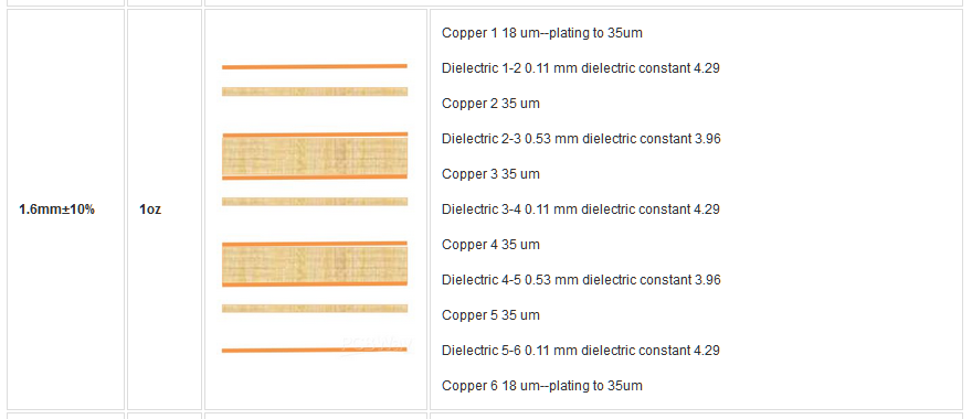
4-layer PCB Stackup for SDRAM
Here is an example of PCB stack-up that I like to use. A 5 mil wide trace on signal layer acts like a ~50 ohm transmission line.
Advertisement (third-party):
The problem with STM32 pinout
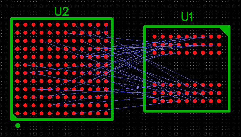
Let’s face it, most BGA STM32 chips have terrible BGA SDRAM interface pinouts. The pins are scattered all over the grid and need to be routed to the appropriate SDRAM balls, which are planned in a JEDEC compliant manner. This tends to make STM32 SDRAM PCB layout much more difficult on a 4-layer board. A 6-layer board has to be used for good layout.
Note that bit and byte swapping rules will apply as usual when routing SDRAM chip lines. You can read more about SDRAM bit and byte swapping.
Routing connections between SDRAM and STM32 can be tricky
Traces and length matching
With the STM32 family of devices, most of the MCUs operate to a maximum of 180 MHz. The maximum FSMC or external memory controller clock rate is half of that, i.e. 90 MHz.
Certain variants like the STM32H7 series are high performance MCUs that can be clocked as fast as 400 MHz. The resulting synchronous external memory clock rate can be 200 MHz.
Here are the rules you need to keep in mind when routing STM32 SDRAM interface lines:
A square wave frequency of 200 MHz contains significant high frequency components as high as 1 GHz. All high speed routing layout rules need to be followed. No hard bends, no stubs on traces and no broken ground plane under any trace.
The trace impedance matters. Datasheet of IS42S16400J, an SDRAM chip compatible with STM32, uses 50 ohms load for deriving its IO characteristics. Trying to achieve roughly 50 ohms characteristic impedance on all traces is a good idea to prevent reflection of signals. While this is not absolutely important, it is important to use the same trace width for all traces to maintain uniform line impedance across all SDRAM signal lines.
Trace to trace clearance should be kept to a minimum of 12 mils. 25 mils is recommended. Avoid parallel meanders if possible to reduce crosstalk.
All signal lines must be referenced to the clock line for length matching as all signals are valid at the rising edge of the clock. All signal lines should be matched to within +/- 400 mils of the clock trace. If multiple clock signals are routed, they must be matched to within +/- 20 mil of each other to prevent clock skew.
Consult the AC timing section of the SDRAM datasheet to find out the maximum allowable skew across signal lines. 0.15mm of unmatched length causes ~1ps of skew. 50ps of skew is acceptable in most STM32 SDRAM PCB layouts, but lower the skew – the better it is.
Try not to push your luck to the boundary with inconsistent layout and length matching. While it might work most of the time, you may have data corruption as temperature swings around the system because propagation time and skew change based on temperature.
Advertisement (third-party):
Have Something to Say? Feel free to ask away via the Quick Contact form in the sidebar, or leave a comment below.