
LAST UPDATED: October 26, 2026
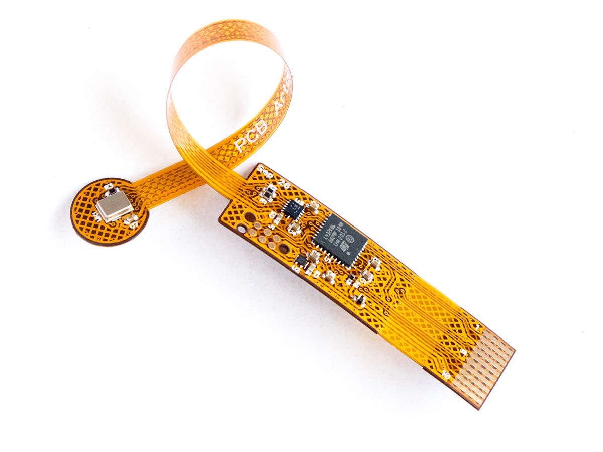
The PCBA-DBM-FLEX-Oct is a flexible PCB-based compact, low-power digital sound level sensor that brings the capability of a professional handheld integrating sound level meter with octave band analysis to embedded systems.
It connects to any host or microcontroller over a standard I2C bus and continuously computes calibrated sound level parameters entirely on board.
The module performs real-time sampling, filtering, A/C/Z frequency weighting, time weighting, Leq integration, peak detection, third octave and octave band analysis, and level history logging. The host simply reads decibel values from I2C registers to obtain this data.
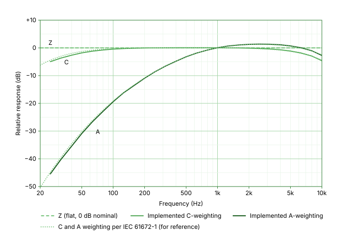
The module has been designed with reference to IEC 61672-1 Class 2 specifications (not certified or type approved), including frequency weighting accuracy, toneburst response, and level decay slopes. It is ideal for systems where a certified instrument is not required but readings must agree with commercial Class 2 sound level meters.
For octave band analysis, the module filters have been designed with reference to IEC 61260-1 Class 2 specifications (not certified or type approved).
Thanks to the tiny measurement microphone head with adhesive for port sealing, the microphone can be mounted inside a ½-inch barrel to obtain a measurement setup that can be calibrated with standard sound meter calibrators.
Features
- Microphone fits in ½-inch barrels
- Sound parameter readings with reference to IEC 61672-1 Class 2*
- Octave band readings with reference to IEC 61260-1 Class 2*
- High accuracy: ±1dB at 1 kHz, 94 dB SPL
- Wide measurement range: 27 dB to 130 dB
- Two decimal points of reading resolution
- Simultaneous A-, C-, and Z- weighted sound levels
- Time weighted levels: Fast, Slow and Custom
- LAeq, LCeq, LZeq with Fast and Slow windows
- LApk, LCpk, LZpk peak level tracking
- Level history: 60 seconds, 60 minutes, 12 hours
- Third-Octave and Octave band spectrum analyzer
- 400 kHz I2C interface
- Active Mode: 7.6 mA @ 3.3V
Sleep Mode: 10 µA @ 3.3V - Factory-checked to ensure accuracy
- Min/Max tracking, several level interrupt sources
- Noise exposure time statistics
Applications
- Industrial and workplace noise monitoring
- Smart city and environmental sensor networks
- IoT nodes with ESP32, Raspberry Pi, Arduino, etc.
- Battery-powered noise loggers
- Smart Home appliances
- Venue sound monitors (classrooms, hospitals, etc.)
Table of Contents
Pin Configuration and Functions

| Pin | Name | Type | Description |
|---|---|---|---|
| 1 | GND | Power | Power ground |
| 2 | GPIO1 | I/O | Reserved |
| 3 | GPIO2 | I/O[2] | Reserved |
| 4 | USB D- | I/O | Reserved |
| 5 | USB D+ | I/O | Reserved |
| 6 | GND | Power | Power ground |
| 7 | SDA | I/O[1][2] | I2C interface SDA |
| 8 | SCL | I/O[1][2] | I2C interface SCL |
| 9 | INT | O[1][2] | Interrupt output (active-low) |
| 10 | VDD | Power | Power supply |
[1] Open-drain pin; pull-ups must be added as per host device requirements
[2] 5V tolerant pin
Mechanical Dimensions
The module is based on a 0.11 mm thick flexible PCB substrate. The polyimide stiffener results in a total PCB thickness of 0.3 mm at the gold pad contact area.
This allows the module to be plugged into hundreds of standard off-the-shelf 10-pin, 1 mm pitch FPC top-contact type connectors.

Electrical Characteristics
Absolute Maximum Ratings
Stresses beyond those listed below may cause permanent damage to the device.
These are stress ratings only and functional operation of the device at these conditions is not implied. Exposure to the absolute maximum ratings conditions for extended periods may affect device reliability.
| Parameter | Min | Typ | Max | Unit |
|---|---|---|---|---|
| Supply Voltage (VDD) | -0.3 | – | 3.6 | V |
| Voltage on SCL and SDA Pins | -0.3 | – | Min (VDD + 3.6, 5.5V) | V |
| Voltage on INT Pin | -0.3 | – | Min (VDD + 3.6, 5.5V) | V |
| Sink Current by any I/O | – | – | 10 | mA |
| Storage Temperature | -55 | – | +100 | °C |
| Sound Pressure Level | – | – | 160 | dB SPL |
Recommended Operating Conditions
| Parameter | Min | Typ | Max | Unit |
|---|---|---|---|---|
| Supply Voltage (VDD) | 1.70 | – | 3.6 | V |
| Voltage on SCL and SDA Pins (VDD ≥ 1.8V) | -0.3 | – | 5.4 | V |
| Voltage on INT Pin (VDD ≥ 1.8V) | -0.3 | – | 5.4 | V |
| Operating Temperature | -40 | – | 85 | °C |
Power Consumption
Current consumption does not depend on acoustic input signal characteristics or loudness.
Average current consumption in various operating modes at TA = 25°C are listed below.
| Parameter | Min | Typ | Max | Unit |
|---|---|---|---|---|
| Active Mode Current (average), VDD = 1.8V | – | 7.6 | – | mA |
| Active Mode Current (average), VDD = 3.3V | – | 7.6 | – | mA |
| Sleep Mode Current (average), VDD = 1.8V | – | 8 | – | µA |
| Sleep Mode Current (average), VDD = 3.3V | – | 10 | – | µA |
The module contains a total of 15 µF in decoupling capacitors on VDD. In ultra-low power applications, it may be important to consider inrush limiting if the system power supply cannot withstand a power-up inrush current of 80 mA for 0.2 milliseconds.
I2C Interface
| Parameter | Min | Typ | Max | Unit |
|---|---|---|---|---|
| Clock Speed | – | 100 | 400 | kHz |
| SCL and SDA Pull-ups | 1 | 4.7 | 10 | kΩ |
| I2C Activation Time after Reset/Power-on | – | 80 | 100 | ms |
| Valid Acoustic Data after Reset/Power-on | – | 100 | 120 | ms |
| Reading Update Rate (all parameters) | – | 62.5 | – | Hz |
Acoustic Characteristics
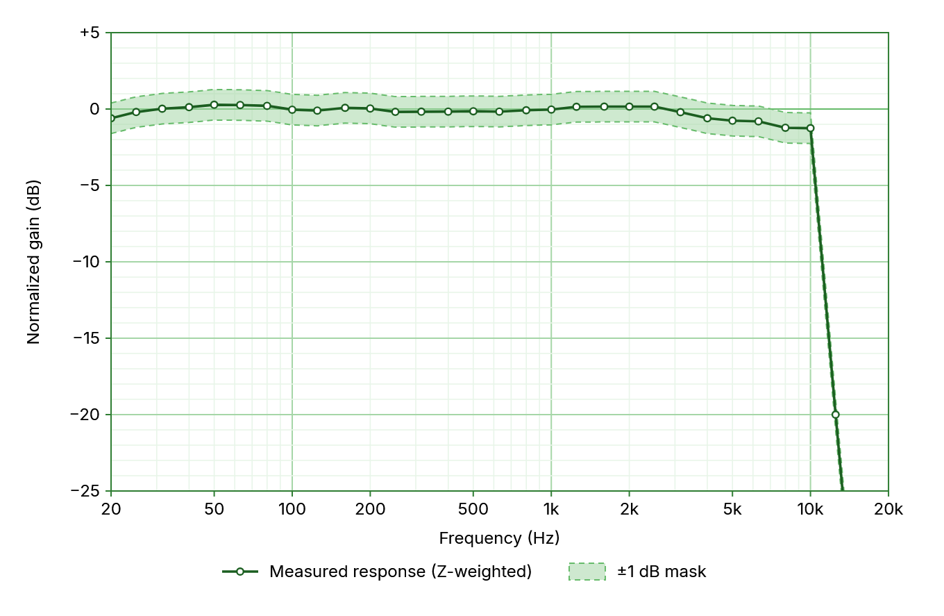
Characteristics listed here are measured with 1 kHz sine tone at TA = 25°C, VDD = 3.3V, RH = 50% unless noted otherwise.
Measurement Characteristics
| Parameter | Min | Typ | Max | Unit |
|---|---|---|---|---|
| Accuracy (1 kHz, 94 dB SPL Reference) | -1 | – | +1 | dB |
| Reading Resolution | – | 0.01 | – | dB |
| Noise Floor (A-weighted) | – | 26 | – | dBA SPL |
| Noise Floor (C-weighted) | – | 34 | – | dBC SPL |
| Noise Floor (Z-weighted) | – | 37 | – | dBZ SPL |
| Linear Operating Range (A-weighted) | 30 | – | 130 | dB SPL |
| Acoustic Overload Point (A-weighted) | – | 131 | – | dB SPL |
| Time Weighting | 1 | – | 65,535 | ms |
| Directionality | – | Omni | – | – |
Sampling Characteristics
| Parameter | Min | Typ | Max | Unit |
|---|---|---|---|---|
| Sampling rate | – | 32.0 | – | kHz |
| Sampling rate drift (TA = 0°C – 85°C) | -1 | – | 1 | % |
| Sampling rate drift (TA = -40°C – 85°C) | -2 | – | 1 | % |
| Flat response range (Under 2 dB error) | 20 | – | 10,000 | Hz |
| DC blocking filter | – | Yes | – | – |
| High-pass filter cutoff (-3 dB point) | – | 8 | – | Hz |
| Stop-band attenuation | 60 | – | – | dB |
Time-Weighting Characteristics
Time weighting behavior has been verified against IEC 61672-1 decay rates specified for Fast and Slow settings. Measured level decay after signal removal is tabulated below and matches the required exponential decay.
| Parameter | Min | Typ | Max | Unit |
|---|---|---|---|---|
| Decay Rate, TAVG = 125 ms | – | 34.7 | – | dB/s |
| Decay Rate, TAVG = 1000 ms | – | 4.3 | – | dB/s |
Third-Octave Filter Characteristics
The module implements a filter for every third-octave band based on its center frequency (base-10 system) and gain skirt shaped by IEC 61260-1 Class 2 guidelines. The filter characteristics are documented in this section. Note that the filter response simply denotes the response of the signal processing chain and does not include the microphone frequency response tolerance for that frequency band.
The exact filter responses and implementation with respect to IEC 61260-1 Class 2 tolerance is shown in Appendix A: Third-Octave Band Filter Response Characteristics.
| No. | Nominal Frequency (Hz) | Exact Frequency (Hz) | Signal-path Group Delay (ms) |
|---|---|---|---|
| 1 | 20 | 19.953 | 331.6 |
| 2 | 25 | 25.119 | 294.2 |
| 3 | 31.5 | 31.623 | 264.3 |
| 4 | 40 | 39.811 | 165.7 |
| 5 | 50 | 50.119 | 147.0 |
| 6 | 63 | 63.096 | 132.0 |
| 7 | 80 | 79.433 | 82.7 |
| 8 | 100 | 100.000 | 73.3 |
| 9 | 125 | 125.893 | 65.8 |
| 10 | 160 | 158.489 | 41.1 |
| 11 | 200 | 199.526 | 36.4 |
| 12 | 250 | 251.189 | 32.6 |
| 13 | 315 | 316.228 | 20.3 |
| 14 | 400 | 398.107 | 17.9 |
| 15 | 500 | 501.187 | 16.0 |
| 16 | 630 | 630.957 | 9.9 |
| 17 | 800 | 794.328 | 8.7 |
| 18 | 1000 | 1000.000 | 7.7 |
| 19 | 1250 | 1258.925 | 4.6 |
| 20 | 1600 | 1584.893 | 4.1 |
| 21 | 2000 | 1995.262 | 3.6 |
| 22 | 2500 | 2511.886 | 2.0 |
| 23 | 3150 | 3162.278 | 1.7 |
| 24 | 4000 | 3981.072 | 1.5 |
| 25 | 5000 | 5011.872 | 0.7 |
| 26 | 6300 | 6309.573 | 0.6 |
| 27 | 8000 | 7943.282 | 0.5 |
Application Information
The module supports several connection configurations for maximum flexibility. It is important to connect the module properly to ensure performance and achieve low power consumption.
Powering the Module
It is important to ensure that the module is supplied with regulated VDD clean of switching noise in the measurement audio frequency range. The module uses a built-in ultra-low dropout 1.8V regulator to power the microphone. When VDD is higher than 1.8V, the internal LDO can produce cleaner power supply for the microphone. In applications using 1.8V supply voltage, it is important to ensure clean power supply at the source itself.
The internal LDO output regulation is stable down to 1.7V, which ensures there are no quiescent current glitches or output noise when operating at VDD = 1.8V.
Ground return paths must be short and low impedance. For design and layout purposes, the module should be treated as a mixed signal device.
Hardware Connection Guidelines
When integrating the module into your custom hardware design, design guidelines and constraints specific to each pin are listed below.
- IMPORTANT: Accidentally reversing power supply polarity or feeding VDD higher than 3.6V will cause permanent damage to the module.
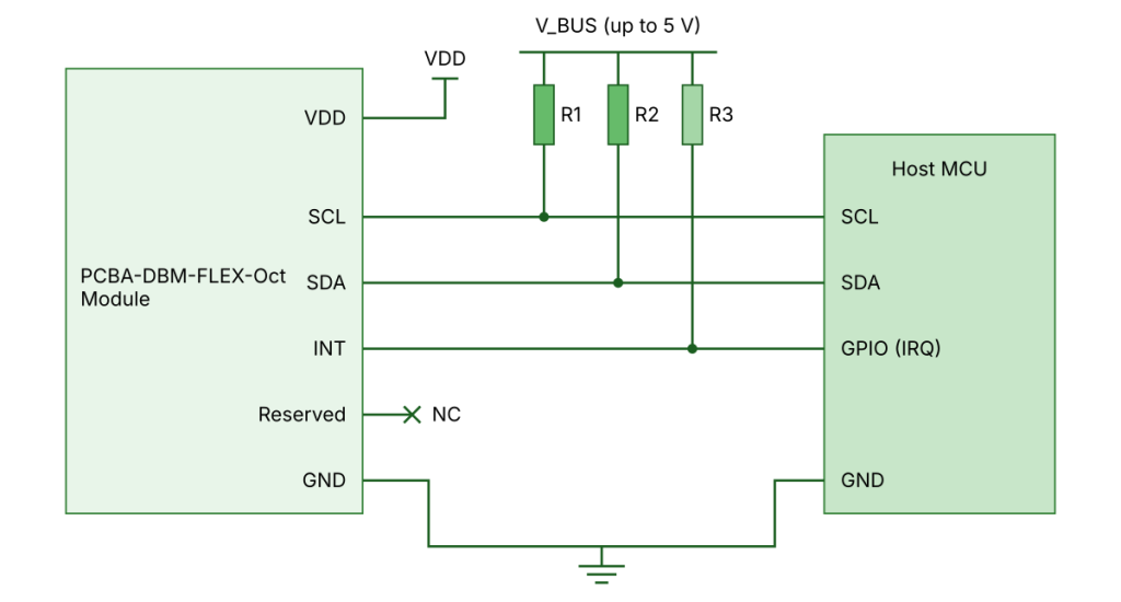
- SCL and SDA are open-drain, 5V tolerant I2C bus lines. These pins may be connected directly to a bus using voltage levels higher than module VDD. External pull-ups must be supplied for reliable communication.
- INT pin is an open-drain, 5V tolerant, active-low interrupt output signal. An external pull-up is needed to use this pin.
- For using 400 kHz I2C clock rate, 4.7K pull-ups are recommended. If the module is connected using a wire cable, total length under 15 cm is preferable.
- Reserved pins should be left unconnected.
Sleep Mode Current Consumption
To ensure that the module can achieve the extremely low sleep current consumption listed in this datasheet, the pull-ups on SCL and SDA lines must be kept active in sleep mode. If SCL and SDA are floated when the module is in sleep mode, power consumption rises significantly as the module tries to decode noise in the signal lines hunting for an address match.
When the module enters sleep mode, the INT pin is floated by the module.
If the application requires SCL and SDA pull-ups to be disabled in sleep mode, it is recommended to switch off the module power supply using a PMOS power switch.
When the module VDD is switched off, the system design should ensure that no other pins are powered up or pulled up. Doing so carries the risk of exceeding maximum voltage specifications on SCL, SDA, or INT pins on a 5V bus.
Operational Overview
The PCBA-DBM-FLEX-Oct integrates a low-power MEMS microphone and an Arm® Cortex®-M4F MCU for digital signal processing. The module processes sound level information in real time and is configured as an I2C slave with a fixed slave address for interfacing with a host system.
When the sensor powers up, it initializes its DSP pipeline and starts processing audio data. It is ideal for the host to wait for 120 ms after power is supplied before attempting communication with the sensor.
To ensure accurate audio data analysis, the module applies corrections to the microphone on board and compensates for its frequency response and DC bias to obtain a clean Z-weighted audio stream. Similarly, C- and A- weighted streams are also obtained using filters designed with reference to IEC 61672-1 guidelines. These streams are analyzed to obtain measurement parameters simultaneously.
In a parallel path, the audio data is also processed using filters designed with reference to IEC 61260-1 to obtain third-octave and octave band audio streams and their corresponding levels.
The acoustics data calculated above is presented via I2C registers with a fixed update rate of 62.5 Hz (once every 16 ms). It is important to note that the sensor performs real-time operations on the audio stream, and excessive I2C communication can starve the module of CPU time and cause a reset. There is sufficient headroom for the host MCU to read all parameters once within the 16 ms refresh period, but unnecessary duplicate register access should be avoided.
At any time, the host MCU may clear any tracked parameters such as minimum/maximum level records and peak trackers. Whenever such an operation is performed via the RESET register, data registers may still retain their current value until the next update cycle or read 0 briefly until the next update cycle puts a valid value in them. It is recommended that the host MCU not use tracking register values for at least 16 ms after performing a reset operation. Specific information on this behavior is available in the Detailed Feature Description section.
Detailed Feature Description
The PCBA-DBM-FLEX-Oct sensor offers a variety of features that are discussed in detail below. For convenience, the features described follow the same sequence as the device I2C registers.
Module Type/Version Detection
Every PCB Artists sound level sensor module presents a module identifier via Register 0 (VERSION). The VERSION register value can be used to identify which sensor is connected to a host MCU. For PCBA-DBM-FLEX-Oct modules, the VERSION register will always read 0xAD, where 0xA represents the flexible module form factor, and 0xD represents the “Octave Analyzer” feature set.
Minor firmware revision identification can be done by reading the value of SCRATCH register.
Sensor Identification
Every sensor module comes pre-programmed with a 32-bit “unique ID” that may be used as an identifier for that sensor module. The UID is not sequential.
Note that the UID is only 32-bits and is therefore not guaranteed to be unique for every sensor ever manufactured. UID may be used to track if a sensor was physically changed and combined with other unique data to form a device identifier. Using the UID alone as a device identifier in large-scale projects is not recommended.
Communication Diagnostics
A scratchpad register (register 0x05) is provided for the host to write any value to the register and then read it back to verify communication. This register also acts as a minor firmware version identifier.
The SCRATCH register can be used to diagnose if the module was accidentally reset due to I2C bus overloading. The host can write a value to the scratch register and periodically check if the value has been changed back to boot-default.
A reset, power cycle, or wake from sleep will always restore the scratchpad register to its default contents.
Frequency Weighting
The module supports simultaneous measurement of A-, C-, and Z-weighted levels. No configuration is needed to enable any weighting system. The host MCU can simply read the appropriate weighted value from device registers.
Accurate weighting filters have been implemented over the range of 20 Hz to 10 kHz with reference to IEC 61672-1 Class 2 guidelines.
Time Weighting
The module implements time weighting as described in IEC 61672-1. Exponential time weighting is applied to the instantaneous sound pressure using the 16-bit time constant determined by TAVG (registers 0x07, 0x08).
LA/LC/LZ readings use this time constant. Octave and third-octave band values also use this for time weighting individual band readings.
TAVG is programmable from 1 ms to 65535 ms. A setting of 1000 is the default value, which is equivalent to “slow“ mode on a sound level meter. Writing 0 to TAVG automatically sets TAVG to 1 ms.
Setting TAVG to 125 ms will be equivalent to “fast” mode on a sound level meter. While the sensor supports TAVG = 35 ms, note that the sensor will not hold on to impulse events like a regular handheld meter with impulse mode does to allow for visual readings. A host using the sensor can easily implement this behavior if required.
Time-weighted outputs with A-, C-, Z- frequency weighting are available via registers LA, LC, and LZ, respectively.
Equivalent Continuous Levels (Leq)
Independent of the TAVG setting, the module computes fixed-window equivalent continuous sound levels.
LAeq/LCeq/LZeq over 125 ms can be read via LXeq_fast registers, and LAeq/LCeq/LZeq over 1 second can be read via LXeq_slow registers.
The LAeq_slow register value is exclusively used to feed the T_OVER and T_UNDER threshold counters and history buffers. The history buffers store 60 seconds of LAeq_slow/LAeq,1s, 60 minutes of LAeq,1min, and 12 hours of LAeq,1hr.
Peak Level Tracking (Lpeak)
LA,peak, LC,peak, and LZ,peak (stored in registers LA_pk, LC_pk, and LZ_pk) are the highest peak sound pressure level sample values observed by the sensor microphone since the last peak reset operation was performed.
In conjunction with other parameters, peak tracking can be used to accurately detect loud, impulsive events.
All peak tracking registers are read-only and can only be cleared using the RESET register.
Maximum and Minimum Level Tracking
The module always tracks the maximum and minimum values of LA, LC, and LZ. The LA_MAX/LC_MAX/LZ_MAX and LA_MIN/LC_MIN/LZ_MIN registers make this data available.
Minimum/maximum tracking registers are read-only and can only be cleared using the RESET register.
Threshold and Noise Exposure Counters
Registers THR_MAX and THR_MIN are threshold registers used to define a level window in decibels. The module always counts the total number of seconds where LAeq_slow has been over THR_MAX or under THR_MIN. Time over THR_MAX is recorded in the 24-bit T_OVER register. Time under THR_MIN is recorded in the 24-bit T_UNDER registers.
Note that the T_OVER and T_UNDER registers roll over to 0 after counting to ~1193 hours (4,294,967 seconds). If these registers are being used in the application, the host should ideally clear these registers at least once every 24 hours. If the host has an accurate clock system, clearing the counters every 1 hour or more often is highly recommended because the module clock can drift and cause errors to accumulate over time.
These registers can only be cleared using the RESET register.
The combination of history registers and T_OVER/T_UNDER counters can be used to determine noise exposure and calculate noise exposure equivalents.
Interrupt Function
Interrupt pin function can be enabled using the CONTROL register. The interrupt pin supports two modes of operation – threshold-based interrupts and fixed-interval interrupt every sixty seconds.
When the interrupt pin is configured to interrupt every 60 seconds, it can be used to wake up the host MCU so that the history registers can be read before any old data point is discarded.
When threshold mode is used, the sensor uses the INT_SRC register to determine which parameter is monitored to generate an interrupt. The value of the parameter set via INT_SRC is compared against threshold registers THR_MAX and THR_MIN. If the value of the target parameter is higher than THR_MAX or lower than THR_MIN, the interrupt pin is activated.
Note that the comparison between the target parameter and THR_MAX/THR_MIN happens once every refresh cycle. This results in an interrupt latency of up to the refresh cycle time period (16 ms in this case).
A pending interrupt can only be cleared by using the RESET register. The INT pin stays low until it is cleared by using the RESET register. Clearing or disabling the interrupt immediately releases the INT pin.
Putting the module in sleep mode automatically releases the INT pin even if it was active when the sleep command was issued.
Synchronous Data Transfer
In applications where the host must be able to read every unique data frame synchronously as soon as registers are refreshed, the interrupt feature and threshold registers can be combined to generate an interrupt every time new data is available.
The host can set THR_MAX to a value lower than the noise floor of the sensor (for example, THR_MAX = 10). This will cause INT to be asserted every time a fresh reading is available. On receiving an interrupt, the host should clear the interrupt using the RESET register and then read required data registers. This sets up a cycle where the host gets a 62.5Hz interrupt-driven synchronous transfer of acoustic parameters.
Note that this approach makes T_OVER register count every second and makes the parameter meaningless.
Sound Level History
The sensor maintains three rolling LAeq history buffers that the host can read at any time. The history buffers are organized in a 60-60-12 structure. The first sixty registers hold the most recent 60 seconds of LAeq,1s values. The next sixty registers hold the most recent 60 minutes of LAeq,1min values. The final twelve registers hold the most recent 12 hours of LAeq,1hr values.
The host can use the antilog of values in history registers to calculate the LAeq over any arbitrary period accurately without having to store and average individual LAeq values continuously. Because the history values are stored as rounded integers, resolution is limited to 1 dB.
History registers are always maintained by the sensor as long as the sensor is in active mode. In low-power applications, the host can enter sleep mode to conserve power while the module records history data. The host can then wake up periodically, read the history data, clear the history buffers via the RESET register, and go back to sleep mode.
Third-Octave Band Analyzer
The sensor measures time-weighted third-octave band sound levels for frequency bands ranging from 20 Hz to 8 kHz. This is useful in applications where spectrum data is required in third-octave band format.
To produce measurements closely comparable to certified handheld meters, the sensor uses third-octave band filters that follow IEC 61260-1 class 2 design guidelines. With filter responses fitted to the specifications and a flat microphone response, the sensor can produce very accurate third-octave band sound levels.
The center frequency points are determined using a base-10 system with G = 103/10 = 1.99526. Nominal frequency vs actual center frequency is tabulated in the Third Octave Filter Characteristics section for reference.
Note that the filter chain used to obtain the third-octave bands introduces varying group delay for constituent frequencies. This group delay depends on the frequency of concern, and the Third Octave Filter Characteristics table lists group delay for each center frequency. The real-world effect of filter group delay is observable when the sensor is subjected to an abrupt and loud “tap” sound. The sensor third-octave band reading will respond with a lag equivalent to the group delay for that frequency.
Octave Band Analyzer
The sensor measures nine time-weighted octave band sound levels for frequency bands ranging from 31.5 Hz to 8 kHz. Nominal frequencies for these bands are 31.5 Hz, 63 Hz, 125 Hz, 250 Hz, 500 Hz, 1 kHz, 2 kHz, 4 kHz, and 8 kHz. This is useful in applications where spectrum data is required in octave band format.
Octave band sound level is calculated from constituent third-octave band magnitudes as outlined in IEC 61260-1 and the filters are therefore compliant with the gain skirts outlined in the standard. The 8 kHz octave band has its own filter instead of relying on constituent third-octave bands because the 10 kHz third-octave band is not implemented.
While the frequency response of filters for all bands follow the IEC 61260-1 class 2 shape, the 8 kHz band follows a steeper attenuation curve past 10 kHz because the module MEMS microphone decimation filter has a cut-off at approximately 10.1 kHz. In practice, this makes little difference to the 8 kHz band sound level because frequencies higher than 10 kHz are already heavily attenuated for that band.
Sleep Mode
In applications where power consumption must be optimized, the module offers a sleep mode that can be entered by writing to the CONTROL register.
During sleep, the module keeps listening for its address and any I2C read or write operation addressing the module will cause the module to acknowledge the transaction and then perform a self-reset to enter regular operation. All registers will be reset to default, and history registers will also be emptied. The transaction that wakes up the module has no meaningful effect because the module immediately self-resets after the first transaction finishes. For consistency, it is recommended that the host perform a module reset via the RESET register or simply read the VERSION register to trigger a wake-up.
To prevent wake-up glitches, the host system must keep SCL and SDA pull-ups active when the module is in sleep mode. If pull-ups must be disabled, the sensor power supply should also be cut off to prevent floating SCL and SDA lines.
I2C Interface and Registers
Device Address and Bus Behavior
The module has a 7-bit I2C address of 0x48 and operates as an I2C slave device.
All common register read/write modes are supported, including multi-byte transfers with address auto-increment. The internal register pointer wraps to 0 after the last register (address 0xFF). Bus clock speeds of 400 kHz and 100 kHz are both supported.
Data Validity
All valid decibel values will always be read as a non-zero number. If a decibel value reads 0, the host should treat that value as “not ready”.
There are several normal situations where a sound level parameter may read as 0. For example, history buffer points that are not yet filled will read 0. Parameters that have been cleared by using the RESET register may read unchanged or 0 before being updated by the sensor in the next update cycle. Many registers may also read 0 immediately after a module reset or power-up until data is available.
Read and Write Sequences
Single Byte Read
I2C Start → Dev Addr | Write → Register Address → I2C Restart → Dev Addr | Read → Read 1 byte → I2C Stop
Single Byte Write
I2C Start → Send Dev Addr | Write → Register Address → Write 1 byte → I2C Stop
Multiple Byte Read
I2C Start → Dev Addr | Write → Register Address → I2C Restart → Dev Addr | Read → Read n bytes → I2C Stop
Multiple Byte Write
I2C Start → Send Dev Addr | Write → Register Address → Write n bytes → I2C Stop
Maximum Data Throughput
In applications that read out all registers every 16 milliseconds, 400 kHz is the required clock speed. Multi-byte read access is the most efficient way to perform reads when multiple consecutive registers need to be fetched.
The module MCU can be overwhelmed by excessively frequent transactions and trigger a self-reset if it is not able to process real-time audio data.
The module has sufficient headroom to safely handle its entire register space being read once within the 16 ms update period. In practice, the host MCU should avoid reading the same register twice within any 16 ms window because the values will not have changed.
Register Page Implementation
The PCBA-DBM-FLEX-Oct exposes many parameters, not all of which can be accommodated within a simple 256-register space.
To make room for parameters like data history, octave, and third-octave band data along with all the other standard sound level measurement parameters, the sensor exposes different “pages” that can be mapped on to the addressable space.
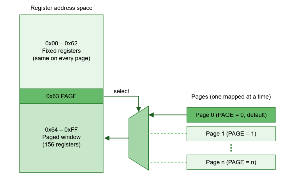
The sensor only implements register paging in the address range of 0x64 – 0xFF. The PAGE register at 0x63 determines which page is mapped to register range 0x64 – 0xFF.
For example, when PAGE = 0, the address range 0x64 – 0xFF read the history value registers. When PAGE = 1, the address range 0x64 – 0xFF now reads back the octave and third-octave band data.
Registers 0x00 – 0x63 are not part of the paging setup and will always refer to the same commonly-used sound level measurement parameters. This makes it easy for the host to always access common parameters without making a page change.
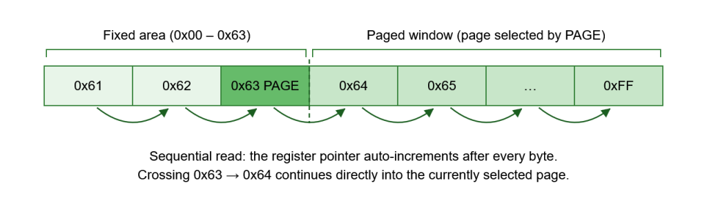
The I2C auto-increment behavior also uses the page set via the PAGE register.
For example, if PAGE = 0, a multi-byte read operation will auto-increment from register 0x63 to page0_0x64. However, if PAGE = 1, a multi-byte read operation will auto-increment from register 0x63 to page1_0x64.
The PAGE register can be written or read at any time.
Register Map
The following table summarizes available registers on the device.
Writing to undocumented registers is not recommended, and reading from them may return undefined values.
| Address | Name | R/W | Reset Value | Description |
|---|---|---|---|---|
| 0x00 | VERSION | R/O | 0xAD | Version Register |
| 0x01 – 0x04 | ID3:ID0 | R/O | – | Unique Device ID |
| 0x05 | SCRATCH | R/W | 0x01 | Scratchpad Register |
| 0x06 | CONTROL | R/W | 0x04 | Control Register |
| 0x07, 0x08 | TAVG | R/W | 0x03, 0xE8 | Weighting Time (milliseconds) |
| 0x09 | RESET | W/O | 0x00 | Reset Register |
| 0x0A, 0x0B | LA | R/O | 0x00 | LA, A-weighted Sound Level (dB SPL) |
| 0x0C, 0x0D | LC | R/O | 0x00 | LC, C-weighted Sound Level (dB SPL) |
| 0x0E, 0x0F | LZ | R/O | 0x00 | LZ, Z-weighted Sound Level (dB SPL) |
| 0x10, 0x11 | LAeq_fast | R/O | 0x00 | LAeq,fast, A-weighted Leq over 125 ms (dB SPL) |
| 0x12, 0x13 | LCeq_fast | R/O | 0x00 | LCeq,fast, C-weighted Leq over 125 ms (dB SPL) |
| 0x14, 0x15 | LZeq_fast | R/O | 0x00 | LZeq,fast, Z-weighted Leq over 125 ms (dB SPL) |
| 0x16, 0x17 | LAeq_slow | R/O | 0x00 | LAeq,slow, A-weighted Leq over 1 s (dB SPL) |
| 0x18, 0x19 | LCeq_slow | R/O | 0x00 | LCeq,slow, C-weighted Leq over 1 s (dB SPL) |
| 0x1A, 0x1B | LZeq_slow | R/O | 0x00 | LZeq,slow, Z-weighted Leq over 1 s (dB SPL) |
| 0x1C, 0x1D | LA_pk | R/O | 0x00 | LA,peak, A-weighted Peak Sound Level (dB SPL) |
| 0x1E, 0x1F | LC_pk | R/O | 0x00 | LC,peak, C-weighted Peak Sound Level (dB SPL) |
| 0x20, 0x21 | LZ_pk | R/O | 0x00 | LZ,peak, Z-weighted Peak Sound Level (dB SPL) |
| 0x22, 0x23 | LA_MAX | R/O | 0x00 | LAmax, Maximum Observed LA (dB SPL) |
| 0x24, 0x25 | LC_MAX | R/O | 0x00 | LCmax, Maximum Observed LC (dB SPL) |
| 0x26, 0x27 | LZ_MAX | R/O | 0x00 | LZmax, Maximum Observed LZ (dB SPL) |
| 0x28, 0x29 | LA_MIN | R/O | 0x00 | LAmin, Minimum Observed LA (dB SPL) |
| 0x2A, 0x2B | LC_MIN | R/O | 0x00 | LCmin, Minimum Observed LC (dB SPL) |
| 0x2C, 0x2D | LZ_MIN | R/O | 0x00 | LZmin, Minimum Observed LZ (dB SPL) |
| 0x2E | THR_MIN | R/W | 45’d | Lower Threshold (dB SPL) |
| 0x2F | THR_MAX | R/W | 85’d | Upper Threshold (dB SPL) |
| 0x30, 0x31, 0x32 | T_OVER | R/O | 0’d, 0’d, 0’d | Time for which LAeq,slow exceeded THR_MAX (seconds) |
| 0x33, 0x34, 0x35 | T_UNDER | R/O | 0’d, 0’d, 0’d | Time for which LAeq,slow was below THR_MIN (seconds) |
| 0x36 … 0x61 | Reserved | – | – | Reserved, do not write. Values read should be discarded. |
| 0x62 | INT_SRC | R/W | 0x00 | Source selection for interrupts via INT pin |
| 0x63 | PAGE | R/W | 0x00 | Register Page Select |
| Address | Name | R/W | Reset Value | Description |
|---|---|---|---|---|
| 0x64 … 0x9F | HISTORY_SEC_n | R/O | 0’d … 0’d | LAeq,1s history, last 60 seconds |
| 0xA0 … 0xDB | HISTORY_MIN_n | R/O | 0’d … 0’d | LAeq,1min history, last 60 minutes |
| 0xDC … 0xE7 | HISTORY_HRS_n | R/O | 0’d … 0’d | LAeq,1hr history, last 12 hours |
| 0xE8 … 0xFF | Reserved | – | – | Reserved, do not write. Values read should be discarded. |
| Address | Name | R/W | Reset Value | Description |
|---|---|---|---|---|
| 0x64 … 0x99 | THIRD_OCT_n | R/O | 0’d … 0’d | LZ,20Hz to LZ,8kHz in third-octave bands, integer and decimal |
| 0x9A … 0x9F | Reserved | – | – | Reserved, do not write. Values read should be discarded. |
| 0xA0 … 0xB1 | OCT_n | R/O | 0’d … 0’d | LZ,20Hz to LZ,8kHz in octave bands, integer and decimal |
| 0xB2 … 0xFF | Reserved | – | – | Reserved, do not write. Values read should be discarded. |
Register Descriptions
Registers available in the PCBA-DBM-FLEX-Oct module are documented below.
VERSION Register
Address: 0x00 · Default value: 0xAD for PCBA-DBM-FLEX-Oct module · Access: Read-Only
| Bit 7 | Bit 6 | Bit 5 | Bit 4 | Bit 3 | Bit 2 | Bit 1 | Bit 0 |
|---|---|---|---|---|---|---|---|
| HW_VER [7:4] | FW_VER [3:0] | ||||||
| Field | Description |
|---|---|
HW_VER [7:4] | Hardware version/type identifier 4-bit hardware type identifier for the sensor, 0xA for flexible modules. |
FW_VER [3:0] | Firmware version/type identifier 4-bit firmware type identifier for the sensor, 0xD for “Octave analyzer” features. |
ID Registers
Address: 0x01, 0x02, 0x03, 0x04 · Default value: – · Access: Read-Only
| Field | Description |
|---|---|
| ID0 (0x01) | Unique Device ID byte 0 |
| ID1 (0x02) | Unique Device ID byte 1 |
| ID2 (0x03) | Unique Device ID byte 2 |
| ID3 (0x04) | Unique Device ID byte 3 |
| ID0:ID3 | Unique Device ID Registers 0x01 through 0x04 form the 32-bit unique sensor ID. |
SCRATCH Register
Address: 0x05 · Default value: 0x01 · Access: Read/Write
| Bit 7 | Bit 6 | Bit 5 | Bit 4 | Bit 3 | Bit 2 | Bit 1 | Bit 0 |
|---|---|---|---|---|---|---|---|
| SCRATCH | |||||||
| Field | Description |
|---|---|
| SCRATCH | Scratchpad register Scratchpad byte for debugging I2C communication link between host and device. Host may read or write any value to this register at any time. The default value is a “(minor) firmware version identifier” for our internal reference. Value 0x01 refers to module firmware released in October 2026. |
CONTROL Register
Address: 0x06 · Default value: 0x04 · Access: Read/Write
| Bit 7 | Bit 6 | Bit 5 | Bit 4 | Bit 3 | Bit 2 | Bit 1 | Bit 0 |
|---|---|---|---|---|---|---|---|
| – | – | – | – | – | INT_MODE | INT_EN | SLEEP |
| Field | Description |
|---|---|
| SLEEP | Sleep Mode Write 1 to enter sleep mode. Writing 0 has no effect. In sleep mode, measurement is paused and I2C remains active to detect further communication. The module wakes up and self-resets to default values on any valid I2C transaction with the module. |
| INT_EN | Interrupt Enable Set this bit to enable interrupt pin function. The module drives the INT pin low when there is a pending interrupt. |
| INT_MODE | Interrupt Mode Write 1 to enable threshold mode. In threshold mode, INT_SRC register sets an interrupt target parameter (default being LA). The target parameter is monitored continuously, and INT pin goes low if the target parameter is outside the bounds set by THR_MIN and THR_MAX registers. When 0, the module drives the INT pin low once every 60 seconds (time window begins when history registers are cleared). |
TAVG Registers
Address: 0x07, 0x08 · Default value: 3’d, 232’d (= 1000’d) · Access: Read/Write
| Field | Description |
|---|---|
| TAVG_H (0x07) | MSB of 16-bit TAVG value |
| TAVG_L (0x08) | LSB of 16-bit TAVG value |
T<sub>AVG</sub> | Weighting Time Constant Weighting time constant (in milliseconds) used for LA, LC, LZ, octave- and third-octave band level calculations. NOTE: TAVG_L (register 0x08) must be written after TAVG_H (register 0x07) for activating the new weighting time. For example, Set TAVG_H = 0, then TAVG_L = 125 for “fast mode” measurement Set TAVG_H = 3, then TAVG_L = 232 “slow mode” measurement |
RESET Register
Address: 0x09 · Default value: 0x00 · Access: Write-Only
| Bit 7 | Bit 6 | Bit 5 | Bit 4 | Bit 3 | Bit 2 | Bit 1 | Bit 0 |
|---|---|---|---|---|---|---|---|
| – | – | SYS_RST | CLR_PEAK | CLR_TSTATS | CLR_HISTORY | CLR_MAX_MIN | CLR_INT |
| Field | Description |
|---|---|
| CLR_INT | Clear interrupt pin Write 1 to clear the active-low interrupt GPIO. |
| CLR_MAX_MIN | Clear max/min data Write 1 to clear LX_MAX and LX_MIN registers. After clearing, max/min registers may read 0 until they are re-populated in the next update cycle. |
| CLR_HISTORY | Clear History Set this bit to clear seconds, minutes, and hours history logging registers. Cleared/empty history registers will read 0. |
| CLR_TSTATS | Clear Time Statistics Write 1 to clear T_OVER and T_UNDER registers. |
| CLR_PEAK | Clear Peak Measurements Write 1 to clear peak (LX_pk) registers. After clearing, peak registers may read 0 until they are re-populated in the next update cycle. |
| SYS_RST | System Reset Write 1 to trigger a soft reset. All registers will be reset back to their power-up defaults. |
LA Registers
Address: 0x0A, 0x0B · Default value: – · Access: Read-Only
| Field | Description |
|---|---|
| Register 0x0A | Integer part of LA |
| Register 0x0B | Decimal part of LA |
| LA | A-weighted sound level in decibels (dB SPL) This pair of registers contain the latest A-weighted and time-weighted (TAVG) sound pressure level observed by the module. This register pair is updated once every refresh period. Value of LA in dB SPL = reg(0x0A) + reg(0x0B)/100 e.g. if reg(0x0A) = 34, reg(0x0B) = 72, LA = 34.72 dB SPL |
LC Registers
Address: 0x0C, 0x0D · Default value: – · Access: Read-Only
| Field | Description |
|---|---|
| Register 0x0C | Integer part of LC |
| Register 0x0D | Decimal part of LC |
| LC | C-weighted sound level in decibels (dB SPL) This pair of registers contain the latest C-weighted and time-weighted (TAVG) sound pressure level observed by the module. This register pair is updated once every refresh period. Value of LC in dB SPL = reg(0x0C) + reg(0x0D)/100 e.g. if reg(0x0C) = 34, reg(0x0D) = 72, LC = 34.72 dB SPL |
LZ Registers
Address: 0x0E, 0x0F · Default value: – · Access: Read-Only
| Field | Description |
|---|---|
| Register 0x0E | Integer part of LZ |
| Register 0x0F | Decimal part of LZ |
| LZ | Z-weighted sound level in decibels (dB SPL) This pair of registers contain the latest Z-weighted and time-weighted (TAVG) sound pressure level observed by the module. This register pair is updated once every refresh period. Value of LZ in dB SPL = reg(0x0E) + reg(0x0F)/100 e.g. if reg(0x0E) = 34, reg(0x0F) = 72, LZ = 34.72 dB SPL |
LAeq_fast Registers
Address: 0x10, 0x11 · Default value: – · Access: Read-Only
| Field | Description |
|---|---|
| Register 0x10 | Integer part of LAeq,fast |
| Register 0x11 | Decimal part of LAeq,fast |
| LAeq,fast | A-weighted equivalent continuous sound level over 125 ms (dB SPL) This pair of registers contain the latest A-weighted Leq value measured over 125 ms. The registers are updated once every refresh period. Value of LAeq,fast in dB SPL = reg(0x10) + reg(0x11)/100 e.g. if reg(0x10) = 34, reg(0x11) = 72, LAeq,fast = 34.72 dB SPL |
LCeq_fast Registers
Address: 0x12, 0x13 · Default value: – · Access: Read-Only
| Field | Description |
|---|---|
| Register 0x12 | Integer part of LCeq,fast |
| Register 0x13 | Decimal part of LCeq,fast |
| LCeq,fast | C-weighted equivalent continuous sound level over 125 ms (dB SPL) This pair of registers contain the latest C-weighted Leq value measured over 125 ms. The registers are updated once every refresh period. Value of LCeq,fast in dB SPL = reg(0x12) + reg(0x13)/100 e.g. if reg(0x12) = 34, reg(0x13) = 72, LCeq,fast = 34.72 dB SPL |
LZeq_fast Registers
Address: 0x14, 0x15 · Default value: – · Access: Read-Only
| Field | Description |
|---|---|
| Register 0x14 | Integer part of LZeq,fast |
| Register 0x15 | Decimal part of LZeq,fast |
| LZeq,fast | Z-weighted equivalent continuous sound level over 125 ms (dB SPL) This pair of registers contain the latest Z-weighted Leq value measured over 125 ms. The registers are updated once every refresh period. Value of LZeq,fast in dB SPL = reg(0x14) + reg(0x15)/100 e.g. if reg(0x14) = 34, reg(0x15) = 72, LZeq,fast = 34.72 dB SPL |
LAeq_slow Registers
Address: 0x16, 0x17 · Default value: – · Access: Read-Only
| Field | Description |
|---|---|
| Register 0x16 | Integer part of LAeq,slow |
| Register 0x17 | Decimal part of LAeq,slow |
| LAeq,slow | A-weighted equivalent continuous sound level over 1 s (dB SPL) This pair of registers contain the latest A-weighted Leq value measured over 1 s. The registers are updated once every refresh period. Value of LAeq,slow in dB SPL = reg(0x16) + reg(0x17)/100 e.g. if reg(0x16) = 34, reg(0x17) = 72, LAeq,slow = 34.72 dB SPL |
LCeq_slow Registers
Address: 0x18, 0x19 · Default value: – · Access: Read-Only
| Field | Description |
|---|---|
| Register 0x18 | Integer part of LCeq_slow |
| Register 0x19 | Decimal part of LCeq_slow |
| LCeq_slow | C-weighted equivalent continuous sound level over 1 s (dB SPL) This pair of registers contain the latest C-weighted Leq value measured over 1 s. The registers are updated once every refresh period. Value of LCeq,slow in dB SPL = reg(0x18) + reg(0x19)/100 e.g. if reg(0x18) = 34, reg(0x19) = 72, LCeq,slow = 34.72 dB SPL |
LZeq_slow Registers
Address: 0x1A, 0x1B · Default value: – · Access: Read-Only
| Field | Description |
|---|---|
| Register 0x1A | Integer part of LZeq,slow |
| Register 0x1B | Decimal part of LZeq,slow |
| LZeq,slow | Z-weighted equivalent continuous sound level over 1 s (dB SPL) This pair of registers contain the latest Z-weighted Leq value measured over 1 s. The registers are updated once every refresh period. Value of LZeq,slow in dB SPL = reg(0x1A) + reg(0x1B)/100 e.g. if reg(0x1A) = 34, reg(0x1B) = 72, LZeq,slow = 34.72 dB SPL |
LA_pk Registers
Address: 0x1C, 0x1D · Default value: – · Access: Read-Only
| Field | Description |
|---|---|
| Register 0x1C | Integer part of LA,peak |
| Register 0x1D | Decimal part of LA,peak |
| LA,peak | A-weighted peak sound level (dB SPL) Maximum, absolute instantaneous A-weighted sound level observed. These registers are updated once every refresh period. Value of LA,peak in dB SPL = reg(0x1C) + reg(0x1D)/100 e.g. if reg(0x1C) = 34, reg(0x1D) = 72, LA,peak = 34.72 dB SPL |
LC_pk Registers
Address: 0x1E, 0x1F · Default value: – · Access: Read-Only
| Field | Description |
|---|---|
| Register 0x1E | Integer part of LC,peak |
| Register 0x1F | Decimal part of LC,peak |
| LC,peak | C-weighted peak sound level (dB SPL) Maximum, absolute instantaneous C-weighted sound level observed. These registers are updated once every refresh period. Value of LC,peak in dB SPL = reg(0x1E) + reg(0x1F)/100 e.g. if reg(0x1E) = 34, reg(0x1F) = 72, LC,peak = 34.72 dB SPL |
LZ_pk Registers
Address: 0x20, 0x21 · Default value: – · Access: Read-Only
| Field | Description |
|---|---|
| Register 0x20 | Integer part of LZ,peak |
| Register 0x21 | Decimal part of LZ,peak |
| LZ,peak | Z-weighted peak sound level (dB SPL) Maximum, absolute instantaneous Z-weighted sound level observed. These registers are updated once every refresh period. Value of LZ,peak in dB SPL = reg(0x20) + reg(0x21)/100 e.g. if reg(0x20) = 34, reg(0x21) = 72, LZ,peak = 34.72 dB SPL |
LA_MAX Registers
Address: 0x22,0x23 · Default value: – · Access: Read-Only
| Field | Description |
|---|---|
| Register 0x22 | Integer part of LAmax |
| Register 0x23 | Decimal part of LAmax |
| LAmax | Maximum observed LA value (dB SPL) Maximum observed LA value. These registers are updated once every refresh period. Value of LAmax in dB SPL = reg(0x22) + reg(0x23)/100 e.g. if reg(0x22) = 34, reg(0x23) = 72, LAmax = 34.72 dB SPL |
LC_MAX Registers
Address: 0x24,0x25 · Default value: – · Access: Read-Only
| Field | Description |
|---|---|
| Register 0x24 | Integer part of LCmax |
| Register 0x25 | Decimal part of LCmax |
| LCmax | Maximum observed LC value (dB SPL) Maximum observed LC value. These registers are updated once every refresh period. Value of LCmax in dB SPL = reg(0x24) + reg(0x25)/100 e.g. if reg(0x24) = 34, reg(0x25) = 72, LCmax = 34.72 dB SPL |
LZ_MAX Registers
Address: 0x26,0x27 · Default value: – · Access: Read-Only
| Field | Description |
|---|---|
| Register 0x26 | Integer part of LZmax |
| Register 0x27 | Decimal part of LZmax |
| LZmax | Maximum observed LZ value (dB SPL) Maximum observed LZ value. These registers are updated once every refresh period. Value of LZmax in dB SPL = reg(0x26) + reg(0x27)/100 e.g. if reg(0x26) = 34, reg(0x27) = 72, LZmax = 34.72 dB SPL |
LA_MIN Registers
Address: 0x28,0x29 · Default value: – · Access: Read-Only
| Field | Description |
|---|---|
| Register 0x28 | Integer part of LAmin |
| Register 0x29 | Decimal part of LAmin |
| LAmin | Minimum observed LA value (dB SPL) Minimum observed LA value. These registers are updated once every refresh period. Value of LAmin in dB SPL = reg(0x28) + reg(0x29)/100 e.g. if reg(0x28) = 34, reg(0x29) = 72, LAmin = 34.72 dB SPL |
LC_MIN Registers
Address: 0x2A,0x2B · Default value: – · Access: Read-Only
| Field | Description |
|---|---|
| Register 0x2A | Integer part of LCmin |
| Register 0x2B | Decimal part of LCmin |
| LCmin | Minimum observed LC value (dB SPL) Minimum observed LC value. These registers are updated once every refresh period. Value of LCmin in dB SPL = reg(0x2A) + reg(0x2B)/100 e.g. if reg(0x2A) = 34, reg(0x2B) = 72, LCmin = 34.72 dB SPL |
LZ_MIN Registers
Address: 0x2C,0x2D · Default value: – · Access: Read-Only
| Field | Description |
|---|---|
| Register 0x2C | Integer part of LZmin |
| Register 0x2D | Decimal part of LZmin |
| LZmin | Minimum observed LZ value (dB SPL) Minimum observed LZ value. These registers are updated once every refresh period. Value of LZmin in dB SPL = reg(0x2C) + reg(0x2D)/100 e.g. if reg(0x2C) = 34, reg(0x2D) = 72, LZmin = 34.72 dB SPL |
THR_MIN Register
Address: 0x2E · Default value: 45’d · Access: Read/Write
| Bit 7 | Bit 6 | Bit 5 | Bit 4 | Bit 3 | Bit 2 | Bit 1 | Bit 0 |
|---|---|---|---|---|---|---|---|
| THR_MIN [7:0] | |||||||
| Field | Description |
|---|---|
| THR_MIN | Lower threshold (dB SPL) Lower bound for the parameter set by INT_SRC for threshold-based interrupt function. Also the lower bound of LAeq,slow for incrementing T_UNDER counter. |
THR_MAX Register
Address: 0x2F · Default value: 85’d · Access: Read/Write
| Bit 7 | Bit 6 | Bit 5 | Bit 4 | Bit 3 | Bit 2 | Bit 1 | Bit 0 |
|---|---|---|---|---|---|---|---|
| THR_MAX [7:0] | |||||||
| Field | Description |
|---|---|
| THR_MAX | Upper threshold (dB SPL) Upper bound for the parameter set by INT_SRC for threshold-based interrupt function. Also the upper bound of LAeq,slow for incrementing T_OVER counter. |
T_OVER Registers
Address: 0x30, 0x31, 0x32 · Default value: – · Access: Read-Only
| Field | Description |
|---|---|
| Register 0x30 | MSB of 24-bit T_OVER counter |
| Register 0x32 | LSB of 24-bit T_OVER counter |
| T_OVER | Total number of seconds for which LAeq,slow exceeded THR_MAX Counts in seconds and rolls back over to 0 on overflow at ~1193 hours (4,294,967 seconds).. These registers are updated once every refresh period. Value of T_OVER in seconds = reg(0x30)*65536 + reg(0x31)*256 + reg(0x32) |
T_UNDER Registers
Address: 0x33, 0x34, 0x35 · Default value: – · Access: Read-Only
| Field | Description |
|---|---|
| Register 0x33 | MSB of 24-bit T_UNDER counter |
| Register 0x35 | LSB of 24-bit T_UNDER counter |
| T_UNDER | Total number of seconds for which LAeq,slow was below THR_MIN Counts in seconds and rolls back over to 0 on overflow at ~1193 hours (4,294,967 seconds). These registers are updated once every refresh period. Value of T_UNDER in seconds = reg(0x33)*65536 + reg(0x34)*256 + reg(0x35) |
INT_SRC Register
Address: 0x62 · Default value: 0x00 · Access: Read/Write
| Bit 7 | Bit 6 | Bit 5 | Bit 4 | Bit 3 | Bit 2 | Bit 1 | Bit 0 |
|---|---|---|---|---|---|---|---|
| INT_SRC [7:0] | |||||||
| Field | Description |
|---|---|
| INT_SRC | Interrupt source selection 0x00: LA 0x01: LC 0x02: LZ 0x03: LAeq,fast 0x04: LCeq,fast 0x05: LZeq,fast 0x06: LAeq,slow 0x07: LCeq,slow 0x08: LZeq,slow 0x09: LA,peak 0x0A: LC,peak 0x0B: LZ,peak 0x10: Octave band LZ,31.5Hz 0x11: Octave band LZ,63Hz 0x12: Octave band LZ,125Hz 0x13: Octave band LZ,250Hz 0x14: Octave band LZ,500Hz 0x15: Octave band LZ,1kHz 0x16: Octave band LZ,2kHz 0x17: Octave band LZ,4kHz 0x18: Octave band LZ,8kHz |
PAGE Register
Address: 0x63 · Default value: 0x00 · Access: Read/Write
| Bit 7 | Bit 6 | Bit 5 | Bit 4 | Bit 3 | Bit 2 | Bit 1 | Bit 0 |
|---|---|---|---|---|---|---|---|
| PAGE [7:0] | |||||||
| Field | Description |
|---|---|
| PAGE | Register page map setting This register determines which page is mapped to registers in the address range 0x64 – 0xFF. |
Page 0: HISTORY_SEC_n (n=0 to 59) Registers
Address: Page 0: 0x64 – 0x9F · Default value: 0’d · Access: Read-Only
| Field | Description |
|---|---|
| Register 0x64 | Most recent LAeq,slow (or LAeq,1s) sample; HISTORY_SEC_0 |
| … | … |
| Register 0x9F | Oldest LAeq,slow (or LAeq,1s) sample; HISTORY_SEC_59 |
| HISTORY_SEC_n | LAeq,1s history, last 60 seconds The sixty HISTORY_SEC_n registers store a queue of the last sixty LAeq,1s values. History registers are shifted every 1 s, with the latest LAeq,1s entry inserted at HISTORY_SEC_0. Oldest value at HISTORY_SEC_59 is discarded. |
Page 0: HISTORY_MIN_n (n=0 to 59) Registers
Address: Page 0: 0xA0 – 0xDB · Default value: 0’d · Access: Read-Only
| Field | Description |
|---|---|
| Register 0xA0 | Most recent LAeq,1min sample; HISTORY_MIN_0 |
| … | … |
| Register 0xDB | Oldest LAeq,1min sample; HISTORY_MIN_59 |
| HISTORY_MIN_n | LAeq,1min history, last 60 minutes The sixty HISTORY_MIN_n registers store a queue of the last sixty LAeq,1min values. History registers are shifted every 1 minute, with the latest LAeq,1min entry inserted at HISTORY_MIN_0. Oldest value at HISTORY_MIN_59 is discarded. |
Page 0: HISTORY_HRS_n (n=0 to 11) Registers
Address: Page 0: 0xDC – 0xE7 · Default value: 0’d · Access: Read-Only
| Field | Description |
|---|---|
| Register 0xDC | Most recent LAeq,1hr sample; HISTORY_HRS_0 |
| … | … |
| Register 0xE7 | Oldest LAeq,1hr sample; HISTORY_HRS_11 |
| HISTORY_HRS_n | LAeq,1hr history, last 12 hours The twelve HISTORY_HRS_n registers store a queue of the last twelve LAeq,1hr values. History registers are shifted every 1 hour, with the latest LAeq,1hr entry inserted at HISTORY_HRS_0. Oldest value at HISTORY_HRS_11 is discarded. |
Page 1: THIRD_OCT_n (n=0 to 29) Registers
Address: Page 1: 0x64 to 0x9F · Default value: 0’d · Access: Read-Only
| Field | Description |
|---|---|
| Registers 0x64, 0x65 | FC = 20 Hz, integer & decimal part of third-octave band sound level (dBZ SPL), respectively |
| Registers 0x66, 0x67 | FC = 25 Hz, integer & decimal part of third-octave band sound level (dBZ SPL), respectively |
| Registers 0x68, 0x69 | FC = 31.5 Hz, integer & decimal part of third-octave band sound level (dBZ SPL), respectively |
| Registers 0x6A, 0x6B | FC = 40 Hz, integer & decimal part of third-octave band sound level (dBZ SPL), respectively |
| Registers 0x6C, 0x6D | FC = 50 Hz, integer & decimal part of third-octave band sound level (dBZ SPL), respectively |
| Registers 0x6E, 0x6F | FC = 63 Hz, integer & decimal part of third-octave band sound level (dBZ SPL), respectively |
| Registers 0x70, 0x71 | FC = 80 Hz, integer & decimal part of third-octave band sound level (dBZ SPL), respectively |
| Registers 0x72, 0x73 | FC = 100 Hz, integer & decimal part of third-octave band sound level (dBZ SPL), respectively |
| Registers 0x74, 0x75 | FC = 125 Hz, integer & decimal part of third-octave band sound level (dBZ SPL), respectively |
| Registers 0x76, 0x77 | FC = 160 Hz, integer & decimal part of third-octave band sound level (dBZ SPL), respectively |
| Registers 0x78, 0x79 | FC = 200 Hz, integer & decimal part of third-octave band sound level (dBZ SPL), respectively |
| Registers 0x7A, 0x7B | FC = 250 Hz, integer & decimal part of third-octave band sound level (dBZ SPL), respectively |
| Registers 0x7C, 0x7D | FC = 315 Hz, integer & decimal part of third-octave band sound level (dBZ SPL), respectively |
| Registers 0x7E, 0x7F | FC = 400 Hz, integer & decimal part of third-octave band sound level (dBZ SPL), respectively |
| Registers 0x80, 0x81 | FC = 500 Hz, integer & decimal part of third-octave band sound level (dBZ SPL), respectively |
| Registers 0x82, 0x83 | FC = 630 Hz, integer & decimal part of third-octave band sound level (dBZ SPL), respectively |
| Registers 0x84, 0x85 | FC = 800 Hz, integer & decimal part of third-octave band sound level (dBZ SPL), respectively |
| Registers 0x86, 0x87 | FC = 1000 Hz, integer & decimal part of third-octave band sound level (dBZ SPL), respectively |
| Registers 0x88, 0x89 | FC = 1250 Hz, integer & decimal part of third-octave band sound level (dBZ SPL), respectively |
| Registers 0x8A, 0x8B | FC = 1600 Hz, integer & decimal part of third-octave band sound level (dBZ SPL), respectively |
| Registers 0x8C, 0x8D | FC = 2000 Hz, integer & decimal part of third-octave band sound level (dBZ SPL), respectively |
| Registers 0x8E, 0x8F | FC = 2500 Hz, integer & decimal part of third-octave band sound level (dBZ SPL), respectively |
| Registers 0x90, 0x91 | FC = 3150 Hz, integer & decimal part of third-octave band sound level (dBZ SPL), respectively |
| Registers 0x92, 0x93 | FC = 4000 Hz, integer & decimal part of third-octave band sound level (dBZ SPL), respectively |
| Registers 0x94, 0x95 | FC = 5000 Hz, integer & decimal part of third-octave band sound level (dBZ SPL), respectively |
| Registers 0x96, 0x97 | FC = 6300 Hz, integer & decimal part of third-octave band sound level (dBZ SPL), respectively |
| Registers 0x98, 0x99 | FC = 8000 Hz, integer & decimal part of third-octave band sound level (dBZ SPL), respectively |
| Registers 0x9A, 0x9B | Reserved |
| Registers 0x9C, 0x9D | Reserved |
| Registers 0x9E, 0x9F | Reserved |
| THIRD_OCT_n | Third-octave frequency band sound level (dB SPL) Time-weighted (over TAVG) and Z-weighted third-octave band sound level in dB SPL. These registers are updated once every 16 ms. |
Page 1: OCT_n (n=0 to 9) Registers
Address: Page 1: 0xA0 to 0xB3 · Default value: 0’d · Access: Read-Only
| Field | Description |
|---|---|
| Registers 0xA0, 0xA1 | FC = 31.5 Hz, integer & decimal part of octave band sound level (dBZ SPL), respectively |
| Registers 0xA2, 0xA3 | FC = 63 Hz, integer & decimal part of octave band sound level (dBZ SPL), respectively |
| Registers 0xA4, 0xA5 | FC = 125 Hz, integer & decimal part of octave band sound level (dBZ SPL), respectively |
| Registers 0xA6, 0xA7 | FC = 250 Hz, integer & decimal part of octave band sound level (dBZ SPL), respectively |
| Registers 0xA8, 0xA9 | FC = 500 Hz, integer & decimal part of octave band sound level (dBZ SPL), respectively |
| Registers 0xAA, 0xAB | FC = 1000 Hz, integer & decimal part of octave band sound level (dBZ SPL), respectively |
| Registers 0xAC, 0xAD | FC = 2000 Hz, integer & decimal part of octave band sound level (dBZ SPL), respectively |
| Registers 0xAE, 0xAF | FC = 4000 Hz, integer & decimal part of octave band sound level (dBZ SPL), respectively |
| Registers 0xB0, 0xB1 | FC = 8000 Hz, integer & decimal part of octave band sound level (dBZ SPL), respectively |
| Registers 0xB2, 0xB3 | Reserved |
| OCT_n | Octave frequency band sound level (dB SPL) Time-weighted (over TAVG) and Z-weighted octave band sound level in dB SPL. These registers are updated once every 16 ms. |
Data Privacy Declaration
This module processes acoustic signals exclusively through on-board digital signal processing techniques that have been developed in-house by PCB Artists OPC Private Limited. Raw acoustic data is processed internally by the module in millisecond frames to derive acoustic parameters and the audio data is immediately discarded. No legible audio data is ever stored on the module.
This module
- Does NOT record or store raw audio in any form
- Does NOT transmit raw audio over any interface
- Does NOT retain any raw audio of length longer than 32 milliseconds
IEC 61672-1 Class 2 and IEC 61260-1 Class 2 Compliance Note
This module has been designed and characterized with reference to IEC 61672-1 Class 2 and IEC 61260-1 Class 2 specifications, including frequency weighting tolerances, toneburst response, time-weighting decay slopes, band frequency response shape, and center frequencies. Internal test results indicate that the module’s measurement accuracy closely follows Class 2 tolerance limits across typical operating conditions.
However, this product has NOT undergone formal third-party certification and does not carry an official IEC 61672-1 Class 2 or IEC 61260-1 Class 2 type approval. The test data presented in this datasheet is provided for reference and characterization purposes only and should NOT be interpreted as a declaration of conformity.
In practical use with proper installation, this sensor will produce readings consistent with handheld Class 2 sound level meters under normal acoustic conditions. This module is intended for indicative measurement, monitoring, and screening applications where certified instrumentation is NOT required.
This sensor is NOT recommended for use in legally binding noise assessments, regulatory enforcement, or any application where type-approved instrumentation is mandated by law.
Accessories
| Reference | Description |
|---|---|
| PCBA-DBM-PM | IP67 sticker acoustic membrane for protecting module microphone from contaminants |
| PCBA-USB-ADAPTER | USB-C adapter module for connecting the sensor to a PC for demo and evaluation |
| PCBA-DBM-FLEX-Qwiic | Adapter board for interfacing flex sensors with a Qwiic system |
Document Change Log
- October 26, 2026: Initial Release
Important Notice and Disclaimer
This document, related resources, and any associated design advice are provided “as is” with no warranties, express or implied, including without limitation any implied warranties of merchantability, fitness for a particular purpose, or non-infringement of third-party intellectual property rights. You are solely responsible for designing, validating, and testing your application and for ensuring that it meets all applicable standards and regulatory requirements. PCB Artists OPC Private Limited shall not be liable for any direct, indirect, incidental, consequential, or special damages arising out of the use of this document or the products it describes. Information in this document is subject to change without notice.
Arm® and Cortex® are registered trademarks of Arm Limited (or its subsidiaries) in the US and/or elsewhere. I²C is a trademark of NXP B.V. All other product names, logos, brands, and trademarks referenced in this document are the property of their respective owners and are used for identification purposes only; their mention does not imply endorsement.
Appendix A: Third-Octave Band Filter Response Characteristics
Please refer to the datasheet PDF for filter frequency response characteristics.