Pinout and Electrical Characteristics
Summary: This page documents the pinout and electrical characteristics for the PCBA-DBM-r3 sound level sensor module.
Pinout
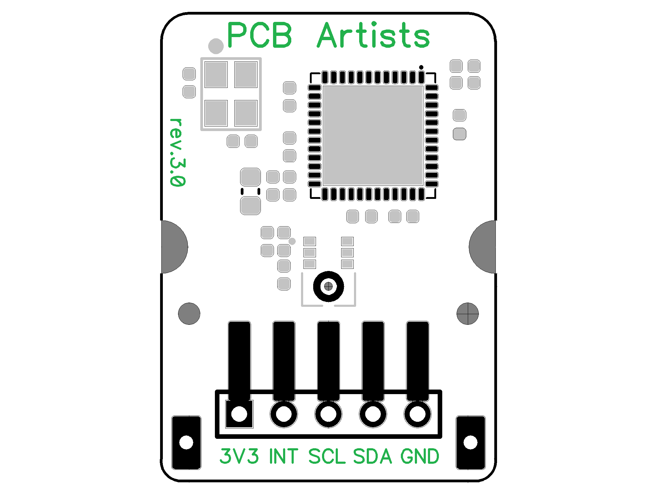
| Pin Name | Description |
| 3V3 | VDD (1.8V or 3.3V) |
| INT | Interrupt output (open-drain, 3.6V tolerant) |
| SCL | I2C SCL (open-drain, 5V tolerant) |
| SDA | I2C SDA (open-drain, 5V tolerant) |
| GND | Supply Ground (VSS) |
Electrical Characteristics
Absolute Maximum Ratings
Exposure to conditions listed as absolute maximum ratings may affect device performance and reliability. Exceeding these conditions may cause permanent damage to the module.
| Parameter | Min | Typ | Max | Unit |
|---|---|---|---|---|
| Supply Voltage (VDD) | -0.3 | – | 3.63 | V |
| Voltage on I2C Pins (SCL and SDA) | -0.3 | – | 5.5 | V |
| Voltage on INT Pin | -0.3 | – | 3.6 | V |
| Storage Temperature | -55 | – | +150 | °C |
| Sound Pressure Level | – | – | 160 | dB |
Recommended Operating Conditions
It is recommended to operate the module under the following conditions for best performance and maximum reliability.
| Parameter | Min | Typ | Max | Unit |
|---|---|---|---|---|
| Supply Voltage (VDD) | 1.71 | – | 3.6 | V |
| Voltage on I2C Pins (SCL and SDA) | -0.3 | – | 5.0 | V |
| Voltage on INT Pin | -0.3 | – | 3.6 | V |
| Operating Temperature Range | -40 | – | +85 | °C |
| I2C Pull-up Resistors | – | 10K | – | kΩ |
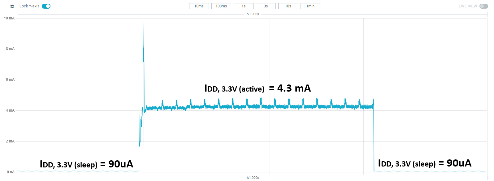
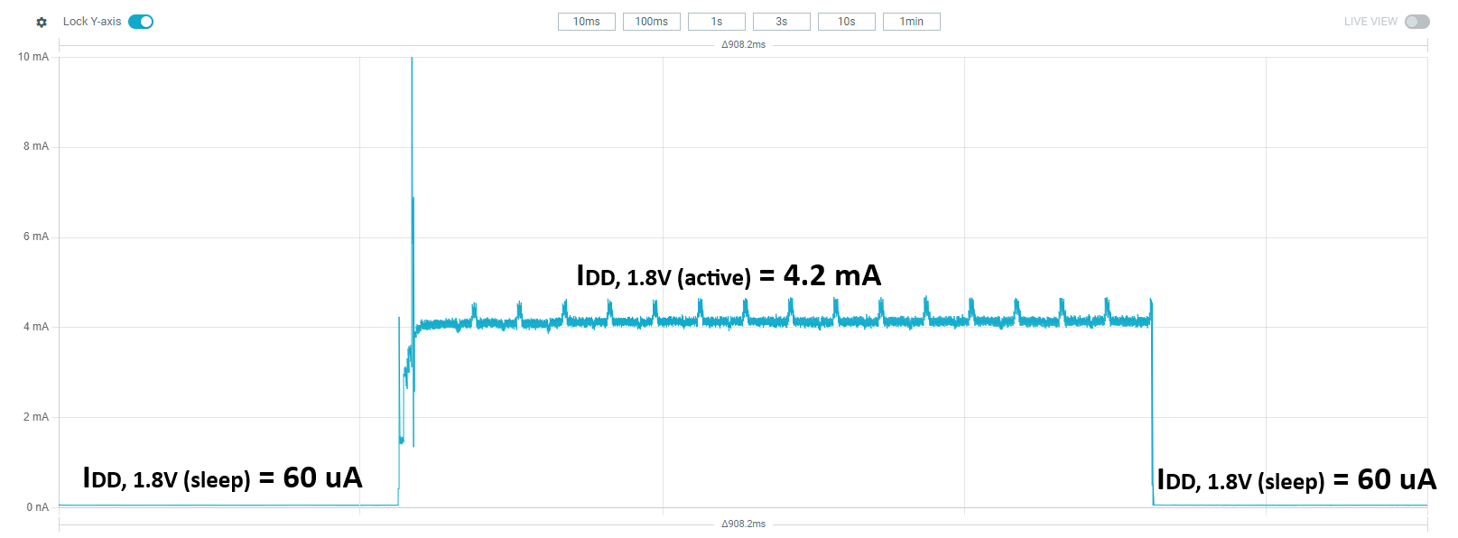
Power Consumption
Power consumption is defined as the current drawn into the VDD pin of the module at an ambient temperature of 25°C.
| Parameter | Min | Typ | Max | Unit |
|---|---|---|---|---|
| Active Mode at VDD = 3.3V (IDD,3V3 (active)) | – | 4.3 | – | mA |
| Active Mode at VDD = 1.8V (IDD,1V8 (active)) | – | 4.2 | – | mA |
| Sleep Mode at VDD = 3.3V (IDD,3V3 (sleep)) | – | 90 | – | uA |
| Sleep Mode at VDD = 1.8V (IDD,1V8 (sleep)) | – | 60 | – | uA |
| Inrush Current (sleep to active mode transition) | 10 | 12 | 15 | mA |
⚠️ A current spike of about ~12 mA is expected when the module wakes up from sleep. The spike may last for a maximum of 60 microseconds.
💡 TIP
Using 1.8V instead of 3.3V can reduce active mode power consumption (in milliwatts) by ~45% and sleep mode power consumption by ~60%.
The following figures show the module transitioning between active and sleep modes at supply voltage of 3.3V and 1.8V.
DC Characteristics
DC characteristics for I/O pins of the module are listed below, assuming an ambient temperature of 25°C.
| Parameter | Min | Typ | Max | Unit |
|---|---|---|---|---|
| I/O Low Level Voltage (VIL) | – | – | 0.3*VDD | V |
| I/O High Level Voltage (VIH) | 0.7*VDD | – | – | V |
| I/O Pin Capacitance | – | 6 | – | pF |
| I/O Pin Sink Current | – | 5 | – | mA |
I²C Interface Specifications
The open-drain I2C interface is capable of withstanding 5V (regardless of the module VDD), making the module compatible with any host that uses an IO voltage of up to 5V without using any additional level converter circuits.
⚠️ Note that the INT pin is open-drain, but not 5V-tolerant.
| Parameter | Typ | Notes |
|---|---|---|
| Supported Clock Speed | 100 kHz | I2C Standard Mode |
| 7-bit Device Address | 0x48 | Can be customized |
| Clock Stretching | Yes | 5 ms (maximum) |
| Time to Ready after Power-up/Reset | 50 ms | – |
Revision History
➤ September 12, 2025
– Initial release
